3.3V Dual LVTTL/LVCMOS-to-Differential
LVPECL Translator
MC100ES60T22
DATA SHEET
The MC100ES60T22 is a low skew dual LVTTL/LVCMOS to differential LVPECL
translator. The low voltage PECL levels, small package, and dual gate design are ideal for
clock translation applications.
Features
•
•
•
•
•
•
D SUFFIX
8-LEAD SOIC PACKAGE
CASE 751-07
280 ps typical propagation delay
100 ps max output-to-output skew
LVPECL operating range: VCC = 3.135 V to 3.8 V
8-lead SOIC and 8-lead TSSOP packages
Ambient temperature range –40°C to +85°C
8-lead SOIC Pb-free package available
Q0
Q0
1
Q1
VCC
DT SUFFIX
8-LEAD TSSOP PACKAGE
CASE 1640-01
7
D0
EJ SUFFIX
8-LEAD SOIC PACKAGE
Pb-FREE PACKAGE
CASE 1640-01
6
D1
8
2
LVPECL
Q1
EF SUFFIX
8-LEAD SOIC PACKAGE
Pb-FREE PACKAGE
CASE 751-07
LVTTL/LVCMOS
3
4
5
ORDERING INFORMATION
Device
GND
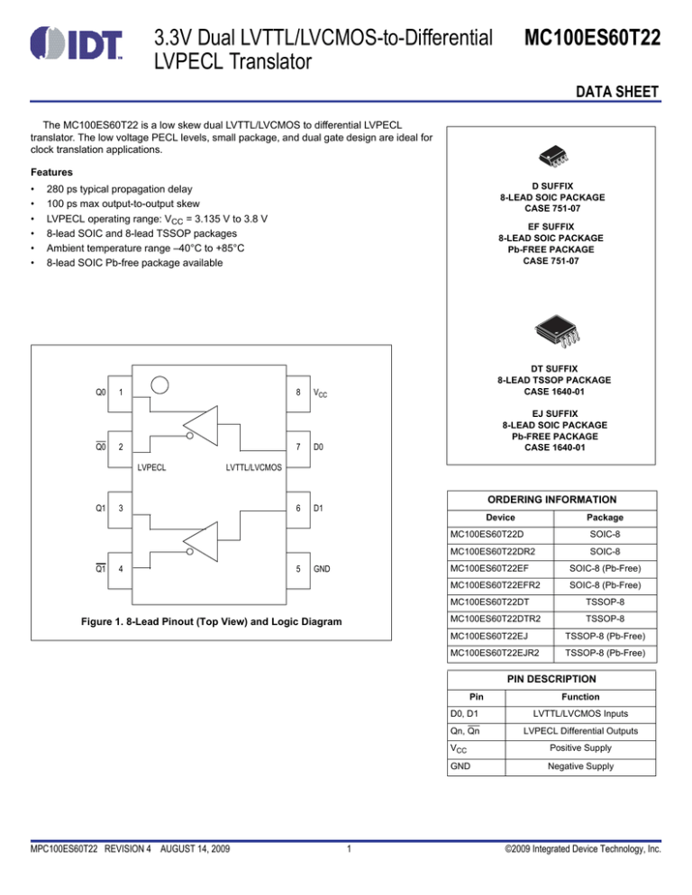
Figure 1. 8-Lead Pinout (Top View) and Logic Diagram
Package
MC100ES60T22D
SOIC-8
MC100ES60T22DR2
SOIC-8
MC100ES60T22EF
SOIC-8 (Pb-Free)
MC100ES60T22EFR2
SOIC-8 (Pb-Free)
MC100ES60T22DT
TSSOP-8
MC100ES60T22DTR2
TSSOP-8
MC100ES60T22EJ
TSSOP-8 (Pb-Free)
MC100ES60T22EJR2
TSSOP-8 (Pb-Free)
PIN DESCRIPTION
Pin
MPC100ES60T22 REVISION 4 AUGUST 14, 2009
1
Function
D0, D1
LVTTL/LVCMOS Inputs
Qn, Qn
LVPECL Differential Outputs
VCC
Positive Supply
GND
Negative Supply
©2009 Integrated Device Technology, Inc.
MPC100ES60T22 Data Sheet
3.3V DUAL LVTTL/LVCMOS-TO-DIFFERENTIAL LVPECL TRANSLATOR
Table 1. General Specifications
Characteristics
Value
Internal Input Pulldown Resistor
75 kΩ
Internal Input Pullup Resistor
75 kΩ
ESD Protection
Human Body Model
Machine Model
> 2000 V
> 200 V
θJA Thermal Resistance (Junction-to-Ambient)
0 LFPM, 8 SOIC
500 LFPM, 8 SOIC
0 LFPM, 8 TSSOP
500 LFPM, 8 TSSOP
190°C/W
130°C/W
185°C/W
140°C/W
Meets or exceeds JEDEC Spec EIA/JESD78 IC Latchup Test
Table 2. Absolute Maximum Ratings(1)
Symbol
Rating
Conditions
Rating
Units
3.9
V
VCC + 0.3
VEE – 0.3
V
V
50
100
mA
mA
Power Supply Voltage
Difference between VCC & VEE
VIN
Input Voltage
VCC – VEE ≤ 3.6 V
Iout
Output Current
Continuous
Surge
TA
Operating Temperature Range
–40 to +85
°C
Storage Temperature Range
–65 to +150
°C
VSUPPLY
TSTG
1. Absolute maximum continuous ratings are those maximum values beyond which damage to the device may occur. Exposure to these
conditions or conditions beyond those indicated may adversely affect device reliability. Functional operation at absolute-maximum-rated
conditions is not implied.
Table 3. DC Characteristics (VCC = 3.135 V to 3.8 V; VEE = 0 V)
-40°C
Symbol
0°C to 85°C
Min
Typ
Max
Min
Typ
Max
Unit
(1)
Output HIGH Voltage
VCC – 1150
VCC – 1020
VCC – 800
VCC – 1200
VCC – 970
VCC – 750
mV
(1)
Output LOW Voltage
VCC – 1950
VCC – 1620
VCC – 1250
VCC – 2000
VCC – 1680
VCC – 1300
mV
Max
Unit
VOH
VOL
Characteristic
1. Outputs are terminated through a 50 Ω resistor to VCC – 2 volts.
Table 4. LVTTL / LVCMOS Input DC Characteristics (VCC = 3.135 V to 3.8 V)
-40°C
Symbol
Characteristic
Condition
Min
Typ
0°C to 85°C
Max
Min
Typ
IIN
Input Current
VIN = VCC
±150
±150
µA
VIK
Input Clamp Voltage
IIN = –18 mA
–1.2
–1.2
V
VIH
Input HIGH Voltage
VCC+0.3
V
VIL
Input LOW Voltage
0.8
V
MPC100ES60T22 REVISION 4 AUGUST 14, 2009
2.0
VCC+0.3
0.8
2
2.0
©2009 Integrated Device Technology, Inc.
MPC100ES60T22 Data Sheet
3.3V DUAL LVTTL/LVCMOS-TO-DIFFERENTIAL LVPECL TRANSLATOR
Table 5. AC Characteristics (VCC = 3.134 V to 3.8 V; VEE = 0 V)
-40°C
Symbol
Characteristic
fmax
Maximum Toggle Frequency
tPLH,
tPHL
Propagation Delay
tSKEW
Skew
Min
25°C
Max
Min
85°C
Typ
Max
1
100
260
part-to-part
tJITTER Cycle-to-Cycle Jitter
400
Output Rise/Fall Times (20% – 80%)
350
Typ
1
100
280
400
100
280
Max
Unit
1
GHz
450
ps
300
350
ps
1
1
1
ps
750
50
Min
300
RMS (1σ)
VoutPP Output Peak-to-Peak Voltage
tr / tf
Typ
350
400
750
350
50
400
Q
50
750
mV
400
ps
D
Driver
Device
Receiver
Device
Qb
Db
50Ω
50Ω
V TT
Figure 2. Typical Termination for Output Driver and Device Evaluation
MPC100ES60T22 REVISION 4 AUGUST 14, 2009
3
©2009 Integrated Device Technology, Inc.
MPC100ES60T22 Data Sheet
3.3V DUAL LVTTL/LVCMOS-TO-DIFFERENTIAL LVPECL TRANSLATOR
PACKAGE DIMENSIONS
PAGE 1 OF 2
CASE 751-07
ISSUE U
8-LEAD SOIC PACKAGE
MPC100ES60T22 REVISION 4 AUGUST 14, 2009
4
©2009 Integrated Device Technology, Inc.
MPC100ES60T22 Data Sheet
3.3V DUAL LVTTL/LVCMOS-TO-DIFFERENTIAL LVPECL TRANSLATOR
PACKAGE DIMENSIONS
PAGE 2 OF 2
CASE 751-07
ISSUE U
8-LEAD SOIC PACKAGE
MPC100ES60T22 REVISION 4 AUGUST 14, 2009
5
©2009 Integrated Device Technology, Inc.
MPC100ES60T22 Data Sheet
3.3V DUAL LVTTL/LVCMOS-TO-DIFFERENTIAL LVPECL TRANSLATOR
PACKAGE DIMENSIONS
2X
3
0.20 C
3.00
1.95
1.5
A
D
8
2
0.60
1
0.60 2.45
B
1.5
3
3.00
H
4.90
B
2X
SEE VIEW C
0.20 C D
VIEW A-A
0.65
0.325
B
8X
0.18
0.13
8
0.38
0.25
0.13
0.23
0.13
BASE METAL
C A-B D
M
0.48 MAX
TOP VIEW
DETAIL "B"
A
0.38
0.25
0.33
0.25
0.25 C
8
SECTION B-B
SEE NOTE 6
DAMBAR PROTRUSION
DETAIL "B"
0.95
0.75
8X
0.10 C
1.10 MAX
SEATING PLANE
0.15
0.05
C
A
SIDE VIEW
4X
15˚
5˚
0.07 MIN
0.25
NOTES:
1. DIMENSIONING AND TOLERANCING PER ASME Y14.5M, 1994.
2. DIMENSIONS ARE IN MILLIMETERS.
3. THIS DIMENSION DOES NOT INCLUDE MOLD FLASH OR PROTRUSIONS
AND ARE MEASURED AT DATUM H, MOLD FLASH OR PROTRUSIONS,
SHALL NOT EXCEED 0.15mm PER SIDE.
4. DIMENSION IS THE LENGTH OF TERMINAL FOR SOLDERING TO A
SUBSTRATE.
5. THE LEAD WIDTH DIMENSION DOES NOT INCLUDE DAMBAR PROTRUSION.
ALLOWABLE DAMBAR PROTRUSION SHALL BE 0.08mm TOTAL IN EXCESS
OF THE LEAD WIDTH DIMENSION AT MAXIMUM MATERIAL CONDITION.
DAMBAR CANNOT BE LOCATED ON THE LOWER RADIUS OR THE LEAD
FOOT. MINIMUM SPACE BETWEEN PROTRUSIONS AND ADJACENT LEAD
TO BE 0.14mm SEE DETAIL "B" AND SECTION B-B.
6. SECTION B-B TO BE DETERMINED AT 0.10 TO 0.25mm FROM THE LEAD TIP.
7. THIS PART IS COMPLIANT WITH JEDEC REGISTRATION MO-187 AA.
8. DATUMS A AND B TO BE DETERMINED DATUM PLANE H.
GAUGE PLANE
SEATING PLANE
6˚
0˚
0.70
0.40
4
4X
15˚
5˚
C
(0.95)
VIEW C
CASE 1640-01
ISSUE O
8-LEAD TSSOP PACKAGE
MPC100ES60T22 REVISION 4 AUGUST 14, 2009
6
©2009 Integrated Device Technology, Inc.
MPC100ES60T22 Data Sheet
6024 Silver Creek Valley Road
San Jose, California 95138
3.3V DUAL LVTTL/LVCMOS-TO-DIFFERENTIAL LVPECL TRANSLATOR
Sales
800-345-7015 (inside USA)
+408-284-8200 (outside USA)
Fax: 408-284-2775
www.IDT.com/go/contactIDT
Technical Support
netcom@idt.com
+480-763-2056
DISCLAIMER Integrated Device Technology, Inc. (IDT) and its subsidiaries reserve the right to modify the products and/or specifications described herein at any time and at IDT’s sole discretion. All information in this document,
including descriptions of product features and performance, is subject to change without notice. Performance specifications and the operating parameters of the described products are determined in the independent state and are not
guaranteed to perform the same way when installed in customer products. The information contained herein is provided without representation or warranty of any kind, whether express or implied, including, but not limited to, the
suitability of IDT’s products for any particular purpose, an implied warranty of merchantability, or non-infringement of the intellectual property rights of others. This document is presented only as a guide and does not convey any
license under intellectual property rights of IDT or any third parties.
IDT’s products are not intended for use in life support systems or similar devices where the failure or malfunction of an IDT product can be reasonably expected to significantly affect the health or safety of users. Anyone using an IDT
product in such a manner does so at their own risk, absent an express, written agreement by IDT.
Integrated Device Technology, IDT and the IDT logo are registered trademarks of IDT. Other trademarks and service marks used herein, including protected names, logos and designs, are the property of IDT or their respective third
party owners.
Copyright 2009. All rights reserved.


