White Paper - DAB in ASICs
advertisement
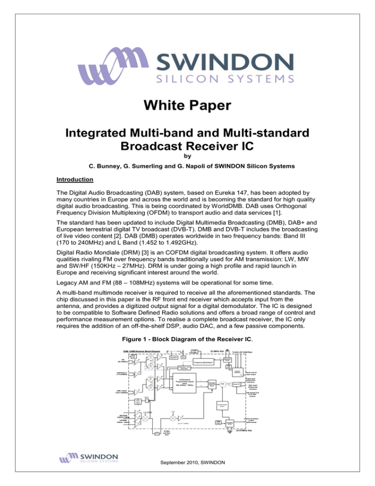
White Paper Integrated Multi-band and Multi-standard Broadcast Receiver IC by C. Bunney, G. Sumerling and G. Napoli of SWINDON Silicon Systems Introduction The Digital Audio Broadcasting (DAB) system, based on Eureka 147, has been adopted by many countries in Europe and across the world and is becoming the standard for high quality digital audio broadcasting. This is being coordinated by WorldDMB. DAB uses Orthogonal Frequency Division Multiplexing (OFDM) to transport audio and data services [1]. The standard has been updated to include Digital Multimedia Broadcasting (DMB), DAB+ and European terrestrial digital TV broadcast (DVB-T). DMB and DVB-T includes the broadcasting of live video content [2]. DAB (DMB) operates worldwide in two frequency bands: Band III (170 to 240MHz) and L Band (1.452 to 1.492GHz). Digital Radio Mondiale (DRM) [3] is an COFDM digital broadcasting system. It offers audio qualities rivaling FM over frequency bands traditionally used for AM transmission: LW, MW and SW/HF (150KHz – 27MHz). DRM is under going a high profile and rapid launch in Europe and receiving significant interest around the world. Legacy AM and FM (88 – 108MHz) systems will be operational for some time. A multi-band multimode receiver is required to receive all the aforementioned standards. The chip discussed in this paper is the RF front end receiver which accepts input from the antenna, and provides a digitized output signal for a digital demodulator. The IC is designed to be compatible to Software Defined Radio solutions and offers a broad range of control and performance measurement options. To realise a complete broadcast receiver, the IC only requires the addition of an off-the-shelf DSP, audio DAC, and a few passive components. Figure 1 - Block Diagram of the Receiver IC. Loop Filter DAB / DRM Receiver Block Diagram 8-bit DAC ML1 regulator FM (88-108MHz) 22.4MHz Xtal 3 wire ctrl interface vco F1 LOHF_ I LOHF_Q Synth.Ref VCXO Frequency Synthesiser ML1 TRIM CTRL Calibration Tone Generator Control Interface DAB Band 3 (174-240MHz) serial readback Serial control data output MB1 LOLF_I LOLF_Q MB1 I Q Analogue Switching Matrix Fsync 10 I/Q Baseband Programmable biquad filters BW: 200Khz - 768Khz ADC Serial I/F Data DAB L Band (1452-1492MHz) Frame sync (Differential interface) data ouput (Differential interface) High Speed CLK from DSP module mixer o/p select AGC detector (prechannel filtered) programmable divider F1x2 LO DRM MW/DRM 520kHz-1.6MHz LW/DRM 150kHz - 280kHz Low IF = 200Khz TRIM CTRL 45 MHz xtal filter (ext) September 2010, SWINDON Sampling VCXO Crystal Oscilllator output (differrential) 24.576MHz Xtal Frequency Conversion To minimize the component count while achieving the required performance, a range of internal frequency conversion methods are used: a) zero IF approach for L Band and Band III b) Low IF for FM c) Double conversion for DRM (and AM). Separate I/Q mixers are provided for L Band; common I/Q mixers for DAB Band III and FM and 2 mixers for the double conversion DRM. All mixer outputs are routed to a programmable baseband filter. In the DRM case the routing is via an external 45MHz bandpass filter to remove signals at the image frequency. The on chip filter can be software configured as an I/Q 768KHz low pass for DAB, an I/Q 200KHz bandpass for FM (centred at 100kHz), or a 20KHz bandpass for DRM (centred at 200KHz). After filtering the signal is digitized in a 10bit ADC. To minimize the number of output data pins, data is multiplexed into a single bit stream with associated start bit. Two crystal maintaining circuits are included for the synthesizer reference and the ADC sampling clock. Receiver IC functionality and dynamic parameter trimming is controlled by the DSP using information made available from the IC via the three wire digital control interface. The DSP monitors both the output of the mixers and the ADC and sets the receiver dynamic range accordingly by adjustment of the LNA, mixer and filter gains. The DSP also adjusts the DAB and FM I/Q amplitude and phase balance to maximize the rejection of signals at the image frequency. Balanced differential circuitry is used throughout excepting the interfaces to the two crystals and to the DRM bandpass filter. The use of differential circuitry has enabled the necessary on chip isolation between the serial digital outputs (2 volt swing) and the various high sensitivity radio inputs (~ 1µV to 3 µV). The IC power consumption is dependent on the radio mode; in digital reception modes it is kept low by only powering up during the required transmission signal burst. LNA The LNA design concept for all bands is shown in Figure 3. A wide dynamic range is achieved by implementing each LNA as a set of four switched amplifiers with fixed gains of 19, 9, -1, and -11 dB. The linearity is higher in the lower gain amplifiers. The LNA achieved a noise figure of 2.2 dB at a gain of 19dB, and an IIP3 of +18.5 dBm at a gain of -11dB. The mixers are straightforward balanced mixers. There are 6 low noise amplifiers (LNA) to cover L Band, Band III, FM, SW, MW, and LW. Figure 3 – LNA Design Concept LNA o/p Amp 1 Amp 2 RF I/P Unity gain buffers Amp 3 Amp 4 Amp 1 Amp 3 Amp 2 Gain Control Inputs September 2010, SWINDON Amp 4 Filtering The baseband filter is a set of eight software configurable Sallen-Key biquad sections. The th DAB and FM filtering is implemented as I/Q 8 order 0.25dB ripple Chebyshev low pass. The th DRM filtering is implemented as a single 8 order 0.25dB ripple Chebyshev bandpass. To overcome the DC offset problems inherent in Zero and Low IF architectures, the filter has an offset cancellation loop. This acts as a single pole high pass transfer function on the filter which completes the FM bandpass filter. By setting the effective high pass to <500Hz, the effect on the DAB OFDM signal is minimal as it only cancels out a null sub-carrier [4]. A fast settle mode allows the offset cancellation loop to settle within 1 time frame of the DAB packet. Figure 4 shows the frequency response of the DAB, FM and DRM filters. In all operating modes the adjacent channel rejection (ACR) performance is heavily influenced by the bandwidth accuracy of the filters. The bandwidth is a function of on chip resistor and capacitor accuracy and varies with process spreads; tuning is achieved using binary trimmed resistors. This is also controlled via the DSP. To aid easy and accurate trimming an in band and an out of band calibration frequency are generated on-chip. Frequency Synthesis The synthesizer controlled PLL uses a single on chip VCO to generate the local oscillator (LO) frequencies for all reception modes. The VCO operates from 2.6GHz to 3.4GHz and is tuned by a combination of switched MIM capacitors and MOS varactors. There are three programmable counters, Figure 5, which together enable a high loop bandwidth and a high comparison frequency (~200kHz) whilst maintaining fine control of the channel centre frequency (DAB 16kHz, FM 10KHz, AM 1KHz). The PLL loop gain is controlled via a programmable charge pump. The reference crystal oscillator can be adjusted over a 100ppm range with a resolution of 0.025ppm using by a combination of switched MIM capacitors and MOS varactors (the ADC reference oscillator is identical). The fine control is required for synchronization to the broadcast reference in the digital reception modes. Figure 6 illustrates the phase noise of the DAB L band LO. Figure 7 demonstrates the low close in LO phase noise required for DRM, -90dBc/Hz has been achieved at 25Hz offset from carrier. Receiver IC Layout The IC has been fabricated on a 0.35um SiGe BiCMOS process, Figure 2. The process features include ~1um thick fourth layer metal, MIM capacitors and bipolar transistors with an Fmax of 50GHz. The die is packaged in an 8x8mm QFN. Figure 2 – IC Layout LNAs and Downconverters September 2010, SWINDON Reference Xstal Oscillator Sampling Xstal Oscillator ADC and Output serialiser VCO and Synthesiser Control logic Baseband Filter References [1] ETSI EN 300 401 v1.3.3 (2001-05), ‘Digital Radio Broadcasting Systems; Digital Audio Broadcasting (DAB) to mobile, portable and fixed receivers’ [2] ETSI TS 102 428 v1.1.1 (2005-06), ‘Digital Audio Broadcasting (DAB); DMB video service; User Application Specification [3] ETSI ES 201980 v2.1.1 (2004-06), ‘Digital Radio Mondiale (DRM); System Specification’ [4] PCT Patent application: SWINDON Silicon Systems The full turnkey mixed signal ASIC solution provider specialising in electronic systems with a core competency on sensor interfaces and ultra low power, enabling products that address widespread needs within Automotive, Industrial, Medical and Consumer applications. Contact us on +44(0) 1793 649400 or sssl@sssl.co.uk September 2010, SWINDON
