Supertex inc.
HV5122
32-Channel Serial to Parallel Converter
With Open Drain Outputs
Features
►► Processed with HVCMOS® technology
►► Output voltages to 225V using a ramped
supply voltage
►► SINK current minimum 100mA
►► Shift register speed 8.0MHz
►► Strobe and enable inputs
►► CMOS compatible inputs
►► Forward and reverse shifting options
►► Hi-Rel processing available
General Description
The HV5122 is a low voltage serial to high voltage parallel converter
with open drain outputs. This device has been designed for use as a
driver for AC electroluminescent displays. They can also be used in
any application requiring multiple output high voltage current sinking
capabilities such as driving inkjet and electrostatic print heads,
plasma panels, vacuum fluorescent, or large matrix LCD displays.
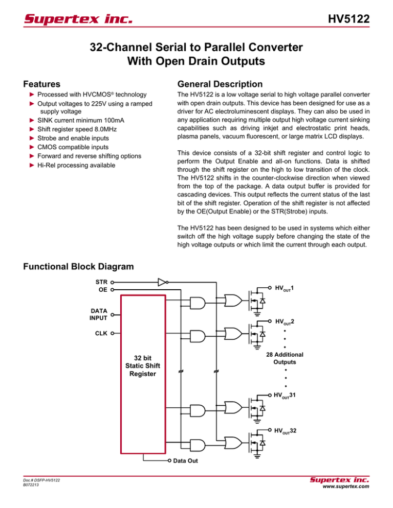
This device consists of a 32-bit shift register and control logic to
perform the Output Enable and all-on functions. Data is shifted
through the shift register on the high to low transition of the clock.
The HV5122 shifts in the counter-clockwise direction when viewed
from the top of the package. A data output buffer is provided for
cascading devices. This output reflects the current status of the last
bit of the shift register. Operation of the shift register is not affected
by the OE(Output Enable) or the STR(Strobe) inputs.
The HV5122 has been designed to be used in systems which either
switch off the high voltage supply before changing the state of the
high voltage outputs or which limit the current through each output.
Functional Block Diagram
STR
OE
HVOUT1
DATA
INPUT
HVOUT2
•
•
•
28 Additional
Outputs
•
•
•
HVOUT31
CLK
32 bit
Static Shift
Register
HVOUT32
Data Out
Doc.# DSFP-HV5122
B072213
Supertex inc.
www.supertex.com
HV5122
Pin Configuration
Ordering Information
Part Number
Package
Packing
HV5122DJ-G*
44-Lead Quad Cerpac
27/Tube
HV5122PG-G
44-Lead PQFP
96/Tray
HV5122PG-G M919
44-Lead PQFP
500/Reel
HV5122PJ-G
44-Lead PLCC
27/Tube
HV5122PJ-G M903
44-Lead PLCC
500/Reel
6
1 44
40
44-Lead Quad Cerpac Chip Carrier
-G denotes a lead (Pb)-free / RoHS compliant package
* Hi-Rel processing available
Absolute Maximum Ratings
Parameter
Value
Supply voltage, VDD
-0.5V to +15V
Supply voltage, VPP
-0.5V to +250V
Logic input levels
44
1
44-Lead PQFP
-0.5V to VDD +0.5V
Ground current1
1.5A
Continuous total power dissipation
Plastic
Ceramic
6
1 44
40
2
1200W
1500W
Operating temperature range
Plastic
Ceramic
-40OC to +85OC
-55OC to +125OC
Storage temperature range
-65OC to +150OC
44-Lead PLCC
Absolute Maximum Ratings are those values beyond which damage to the
device may occur. Functional operation under these conditions is not implied.
Continuous operation of the device at the absolute rating level may affect
device reliability. All voltages are referenced to device ground.
Notes:
1. Duty cycle is limited by the total power dissipated in the package.
2. For operation above 25°C ambient derate linearly to maximum
operating temperature at 20mW/°C for plastic and at 15mW/°C for
ceramic.
Typical Thermal Resistance
Package
θja
44-Lead Quad Cerpac
---
44-Lead PQFP
51OC/W
44-Lead PLCC
37OC/W
Product Marking
Top Marking
Top Marking
YYWW
HV5122DJ
LLLLLLLLLL
Bottom Marking
CCCCCCCCCCC
AAA
Top Marking
YY = Year Sealed
WW = Week Sealed
LLLLLLLLL
L = Lot Number
Bottom Marking C = Country of Origin*
A = Assembler ID*
= “Green” Packaging
CCCCCCCC
YYWW
YY = Year Sealed
WW = Week Sealed
L = Lot Number
C = Country of Origin*
A = Assembler ID*
HV5122PG
*May be part of top marking
AAA
44-Lead Quad Cerpac Chip Carrier
*May be part of top marking
44-Lead PQFP
YYWW AAA
HV5122PJ
LLLLLLLLLL
Bottom Marking
CCCCCCCCCCC
YY = Year Sealed
WW = Week Sealed
L = Lot Number
A = Assembler ID
C = Country of Origin*
= “Green” Packaging
*May be part of top marking
44-Lead PLCC
Packages may or may not include the following marks: Si or
Doc.# DSFP-HV5122
B072213
2
Supertex inc.
www.supertex.com
HV5122
Recommended Operating Conditions
Sym
Parameter
Min
Typ
Max
Units
VDD
Logic voltage supply
10.8
12
13.2
V
HVOUT
High voltage output
-0.3
-
225
V
VIH
High-level input voltage
VDD -2.0
-
VDD
V
VIL
Low-level input voltage
0
-
2.0
V
fCLK
Clock frequency
-
-
8.0
MHz
TA
Operating free-air temperature
Plastic
-40
-
+85
Ceramic
-55
-
+125
C
O
Power-Up Sequence
Power-up sequence should be the following:
1. Connect ground
2. Apply VDD
3. Set all inputs to a known state
Power-down sequence should be the reverse of the above.
Electrical Characteristics (Over recommended operating conditions unless otherwise specified)
DC Characteristics
Sym
Parameter
Min
Max
Units
Conditions
IDD
VDD supply current
-
15
mA
fCLK = 8.0MHz, FDATA = 4.0MHz
IDDQ
Quiescent VDD supply current
-
100
µA
All VIN = 0V
Off-state output current
-
10
µA
All outputs high, all SWS parallel
IIH
High level logic input current
-
1.0
µA
VIH = 12V
IIL
Low level logic input current
-
-1.0
µA
VIL = 0
VDD -1.0V
-
V
IDOUT = -100µA
HVOUT
-
15
Data out
-
1.0
-
-1.5
V
IOL = -100mA
Min
Max
Units
Conditions
-
8.0
MHz
---
IO(OFF)
VOH
High level output data out
VOL
Low level output voltage
VOC
HVOUT clamp voltage
AC Characteristics (V
DD
Sym
V
IHVOUT = +100mA
IDOUT = +100µA
= 12V, TA = 25°C)
Parameter
fCLK
Clock frequency
tW
Clock width, high or low
62
-
ns
---
tSU
Data setup time before CLK falls
25
-
ns
---
tH
Data hold time after CLK falls
10
-
ns
---
tON
Turn-on time, HVOUT from strobe
-
500
ns
RL = 2.0KΩ to 200V
tDHL
Data output delay after H to L CLK
-
100
ns
CL = 15pF
tDLH
Data output delay after L to H CLK
-
100
ns
CL = 15pF
Doc.# DSFP-HV5122
B072213
3
Supertex inc.
www.supertex.com
HV5122
Input and Output Equivalent Circuits
VDD
VDD
HVOUT
DATA
OUT
INPUT
HVIN
GND
GND
GND
Logic Inputs
Logic Data Output
High Voltage Outputs
Switching Waveforms
12V
DATA
IN
Data Valid 1
0V
tSU
CLK
tH
50%
12V
50%
50%
tWH
0V
tWL
DATA
OUT
50%
tDHL
DATA
OUT
tDLH
STR
50%
tON
HVOUT
15V
Function Table
Inputs
Function
Outputs
Data
In
CLK
OE
STR
All on
X
X
X
All off
X
X
Load S/R
H OR L
Output Enable
X
Shift Reg
HV Outputs
Data
Out
1
2...32
1
2...32
L
●
●...●
ON
ON...ON
●
L
H
●
●...●
OFF
OFF...OFF
●
↓
L
H
H or L
●...●
OFF
OFF...OFF
-
H OR L
H
H
H or L
●...●
ON or OFF
●...●
●
Notes:
H = high level, L = low level, X = irrelevant, ↓ = high-to-low transition
● = dependent on previous stage’s state before the last CLK: High-to-low transition
Doc.# DSFP-HV5122
B072213
4
Supertex inc.
www.supertex.com
HV5122
44-Lead PQFP Pin description
Pin
Function
1
HVOUT11
2
HVOUT12
3
HVOUT13
4
HVOUT14
5
HVOUT15
6
HVOUT16
7
HVOUT17
8
HVOUT18
9
HVOUT19
10
HVOUT20
11
HVOUT21
12
HVOUT22
13
HVOUT23
14
HVOUT24
15
HVOUT25
16
HVOUT26
17
HVOUT27
18
HVOUT28
19
HVOUT29
20
HVOUT30
21
HVOUT31
22
HVOUT32
23
DATA OUT
Description
High voltage outputs.
Data output for cascading to the data input of the next device.
24
25
26
N/C
No connect.
27
Output enable input.
28
OE
29
CLK
Data shift register clock. Input are shifted into the shift register on the positive edge of
the clock.
30
GND
Logic and high voltage ground.
31
VDD
Low voltage logic power rail.
32
STR
Strobe.
Doc.# DSFP-HV5122
B072213
When OE is LOW, all HV outputs are forced into a LOW state, regardless of data in
each channel. When OE is HIGH, all HV outputs reflect data latched.
5
Supertex inc.
www.supertex.com
HV5122
44-Lead PQFP Pin description (cont.)
Pin
Function
Description
33
DATA IN
Serial data input. Data needs to be present before each rising edge of the clock.
34
N/C
35
HVOUT1
36
HVOUT2
37
HVOUT3
38
HVOUT4
39
HVOUT5
40
HVOUT6
41
HVOUT7
42
HVOUT8
43
HVOUT9
44
HVOUT10
No connect.
High voltage outputs.
44-Lead PLCC Pin description
Pin
Function
1
HVOUT16
2
HVOUT17
3
HVOUT18
4
HVOUT19
5
HVOUT20
6
HVOUT21
7
HVOUT22
8
HVOUT23
9
HVOUT24
10
HVOUT25
11
HVOUT26
12
HVOUT27
13
HVOUT28
14
HVOUT29
15
HVOUT30
16
HVOUT31
17
HVOUT32
Doc.# DSFP-HV5122
B072213
Function
High voltage outputs
6
Supertex inc.
www.supertex.com
HV5122
44-Lead PLCC Pin description (cont.)
Pin
Function
18
DATA OUT
Function
Data output for cascading to the data input of the next device.
19
20
21
N/C
No connect.
22
Output enable input.
23
OE
24
CLK
Data shift register clock. Input are shifted into the shift register on the positive edge of
the clock.
25
GND
Logic and high voltage ground.
26
VDD
Low voltage logic power rail.
27
STR
Strobe.
28
DATA IN
29
N/C
30
HVOUT1
31
HVOUT2
32
HVOUT3
33
HVOUT4
34
HVOUT5
35
HVOUT6
36
HVOUT7
37
HVOUT8
38
HVOUT9
39
HVOUT10
40
HVOUT11
41
HVOUT12
42
HVOUT13
43
HVOUT14
44
HVOUT15
Doc.# DSFP-HV5122
B072213
When OE is LOW, all HV outputs are forced into a LOW state, regardless of data in
each channel. When OE is HIGH, all HV outputs reflect data latched.
Serial data input. Data needs to be present before each rising edge of the clock.
No connect.
High voltage outputs.
7
Supertex inc.
www.supertex.com
HV5122
44-Lead Quad Cerpac Package Outline (DJ)
.650x.650in body, .190in height (max), .050in pitch
.040 x 45O
D
D1
1 44
6
.035 x 45O
40
.150 max
Note 1
(Index Area)
.075 max
E1
0.25 max
3 Places
E
Vertical Side View
Top View
View B
b1
.025 MIN
A
A2
Seating
Plane
e
A1
b
View B
Horizontal Side View
Note:
1. A Pin 1 identifier must be located in the index area indicated. The Pin 1 identifier can be: a molded mark/identifier; an embedded metal marker; or
a printed indicator.
Symbol
Dimension
(inches)
A
A1
MIN
.155
.090
NOM
.172
.100
MAX
.190
.120
A2
b
b1
D
D1
E
E1
.060
REF
.017
.026
.685
.630
.685
.630
.019
.029
.690
.650
.690
.650
.021
.032
.695
.665
.695
.665
e
.050
BSC
JEDEC Registration MO-087, Variation AB, Issue B, August, 1991.
Drawings not to scale.
Supertex Doc. #: DSPD-44CERPACDJ, Version D090808.
Doc.# DSFP-HV5122
B072213
8
Supertex inc.
www.supertex.com
HV5122
44-Lead PQFP Package Outline (PG)
10.00x10.00mm body, 2.35mm height (max), 0.80mm pitch
D
D1
E1 E
Note 1
(Index Area
D1/4 x E1/4)
44
1
e
b
θ1
Top View
View B
A
A2
Seating
Plane
A1
L
L1
Side View
L2
Gauge
Plane
θ
Seating
Plane
View B
Note:
1. A Pin 1 identifier must be located in the index area indicated. The Pin 1 identifier can be: a molded mark/identifier; an embedded metal marker; or
a printed indicator.
Symbol
MIN
Dimension
NOM
(mm)
MAX
A
A1
A2
b
D
D1
E
E1
1.95*
0.00
1.95
0.30
13.65*
9.80*
13.65*
9.80*
-
-
2.00
-
13.90
10.00
13.90
10.00
2.35
0.25
2.10
0.45
14.15*
10.20* 14.15* 10.20*
e
0.80
BSC
L
0.73
0.88
1.03
L1
L2
1.95
REF
0.25
BSC
θ
0O
3.5O
7O
JEDEC Registration MO-112, Variation AA-2, Issue B, Sep.1995.
* This dimension is not specified in the JEDEC drawing.
Drawings not to scale.
Supertex Doc. #: DSPD-44PQFPPG, Version C041309.
Doc.# DSFP-HV5122
B072213
9
Supertex inc.
www.supertex.com
HV5122
44-Lead PLCC Package Outline (PJ)
.653x.653in body, .180in height (max), .050in pitch
D
D1
.048/.042
x 45O
1
6
44
.150max
.056/.042
x 45O
40
Note 1
(Index Area)
.075max
E
E1
Note 2
e
.020max
(3 Places)
Top View
Vertical Side View
View
B
b1
A
A1
Base .020min
Plane
A2
Seating
Plane
b
Horizontal Side View
R
View B
Notes:
1. A Pin 1 identifier must be located in the index area indicated. The Pin 1 identifier can be: a molded mark/identifier; an embedded metal marker; or
a printed indicator.
2. Actual shape of this feature may vary.
Symbol
Dimension
(inches)
A
A1
A2
b
b1
D
D1
E
E1
MIN
.165
.090
.062
.013
.026
.685
.650
.685
.650
NOM
.172
.105
-
-
-
.690
.653
.690
.653
MAX
.180
.120
.083
.021
.036†
.695
.656
.695
.656
e
.050
BSC
R
.025
.035
.045
JEDEC Registration MS-018, Variation AC, Issue A, June, 1993.
† This dimension differs from the JEDEC drawing.
Drawings not to scale.
Supertex Doc. #: DSPD-44PLCCPJ, Version F031111.
(The package drawing(s) in this data sheet may not reflect the most current specifications. For the latest package outline information go to:
http://www.supertex.com/packaging.html.)
Supertex inc. does not recommend the use of its products in life support applications, and will not knowingly sell them for use in such applications unless it receives
an adequate “product liability indemnification insurance agreement.” Supertex inc. does not assume responsibility for use of devices described, and limits its liability
to the replacement of the devices determined defective due to workmanship. No responsibility is assumed for possible omissions and inaccuracies. Circuitry and
specifications are subject to change without notice. For the latest product specifications refer to the Supertex inc. (website: http//www.supertex.com)
Supertex inc.
©2013 Supertex inc. All rights reserved. Unauthorized use or reproduction is prohibited.
Doc.# DSFP-HV5122
B072213
10
1235 Bordeaux Drive, Sunnyvale, CA 94089
Tel: 408-222-8888
www.supertex.com


