Supertex inc.
HV9801A
Switch Dimmable
LED Driver
Features
General Description
Applications
Through switch dimming, the lamp can be adjusted to four
discrete brightness levels by rapid cycling of the light switch.
The brightness levels are traversed in up and down manner.
Brightness resumes at the highest level when power is
removed for more than a second.
►►
►►
►►
►►
►►
Four level switch dimming
Very accurate current regulator
Output over-current / short circuit protection
IC over-temperature protection
Available in 8L-SOIC and 16L-SOIC packages
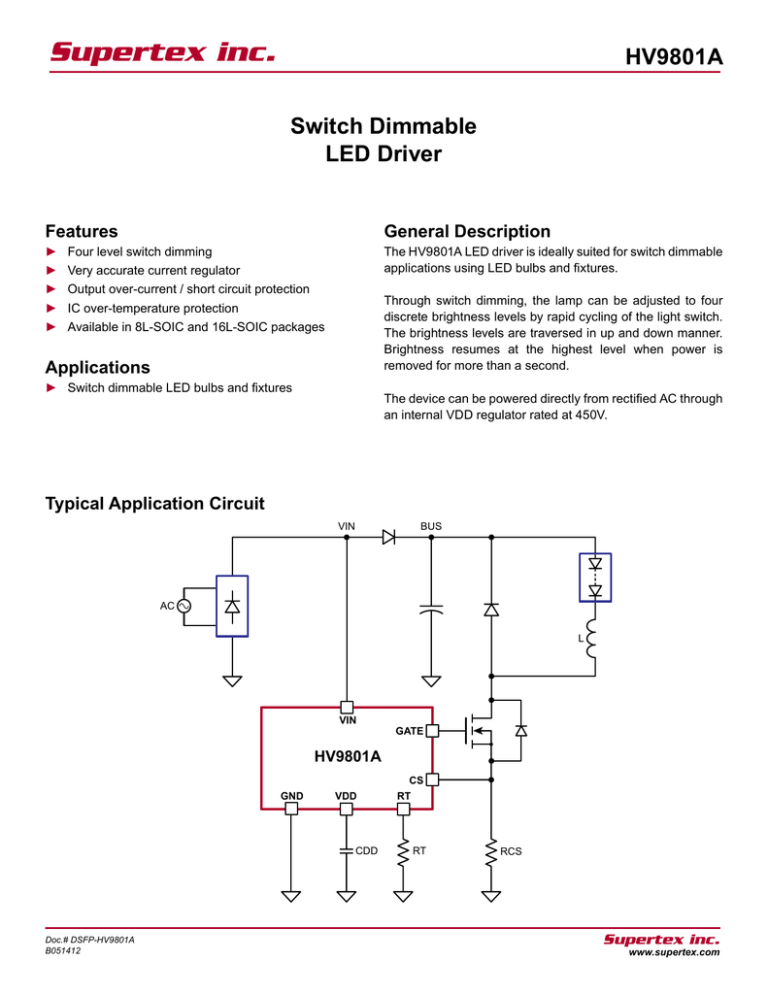
The HV9801A LED driver is ideally suited for switch dimmable
applications using LED bulbs and fixtures.
►► Switch dimmable LED bulbs and fixtures
The device can be powered directly from rectified AC through
an internal VDD regulator rated at 450V.
Typical Application Circuit
VIN
BUS
AC
L
VIN
GATE
HV9801A
CS
GND
VDD
CDD
Doc.# DSFP-HV9801A
B051412
RT
RT
RCS
Supertex inc.
www.supertex.com
HV9801A
Pin Description
Ordering Information
Part Number
Package
Packing
HV9801ALG-G
8-Lead SOIC (Narrow Body)
2500/Reel
HV9801ANG-G
16-Lead SOIC (Narrow Body) 45/Tube
VIN 1
16 DNC
DNC 2
15 DNC
DNC 3
14 RT
CS 4
13 DNC
8 RT
GND 5
12 VDD
CS 2
7 DNC
DNC 6
11 DNC
GND 3
6 VDD
DNC 7
10 DNC
GATE 4
5 DNC
GATE 8
HV9801ANG-G M934 16-Lead SOIC (Narrow Body) 2500/Reel
VIN 1
-G indicates package is RoHS compliant (‘Green’)
8-Lead SOIC (LG)
θja
8-Lead SOIC
101OC/W
16-Lead SOIC
83OC/W
16-Lead SOIC (NG)
Product Marking
Y = Last Digit of Year Sealed
WW = Week Sealed
L = Lot Number
= “Green” Packaging
YWW
9801A
Absolute Maximum Ratings
LLLL
Parameter
Value
VVIN
470V
VVDD
12V
VCS, VLD, VPWMD, VGATE
DNC
Caution! DNC means Do Not Connect!
Typical Thermal Resistance
Package
9
Package may or may not include the following marks: Si or
8-Lead SOIC (LG)
Top Marking
-0.3V to (VVDD +0.3V)
Junction temperature range
-40°C to +150°C
Storage temperature range
-65°C to +150°C
Continuous power dissipation (TA = +25°C)
8-Lead SOIC
16-Lead SOIC
Y = Last Digit of Year Sealed
WW = Week Sealed
L = Lot Number
C = Country of Origin*
A = Assembler ID*
= “Green” Packaging
HV9801ANG
YWW
LLLLLLLL
Bottom Marking
650mW
1000mW
CCCCCCCCC AAA
*May be part of top marking
Stresses beyond those listed under “Absolute Maximum Ratings” may cause
permanent damage to the device. These are stress ratings only, and functional
operation of the device at these or any other conditions beyond those indicated in
the operational sections of the specifications is not implied. Exposure to absolute
maximum rating conditions for extended periods may affect device reliability.
Package may or may not include the following marks: Si or
16-Lead SOIC (NG)
Electrical Characteristics (Specifications are at TA = 25°C, VVIN = 15V unless otherwise noted)
Sym
Description
Min
Typ
Max
Unit
Conditions
Input
VVIN
Input voltage
T
15
-
450
V
---
IVIN
Input current
-
-
1
2
mA
---
Supply current, OTP shutdown
G
-
-
500
μA
---
IVIN,OT
VDD Regulator
VUVLO
Undervoltage lockout threshold
T
6.45
6.70
7.10
V
VVIN rising
ΔVUVLO
Undervoltage lockout hysteresis
-
-
500
-
mV
VVIN falling
Maximum input current, limited by
UVLO
G
3.5
-
-
mA
TA = 25°C
1.5
-
-
mA
TA = 125°C
IUVLO
Notes:
G
Not production tested; guaranteed by design or characterization.
T
Specifications apply over the full operating ambient temperature range of -40°C < TA < +125°C.
Doc.# DSFP-HV9801A
B051412
2
Supertex inc.
www.supertex.com
HV9801A
Electrical Characteristics (Specifications are at T
A
Sym
Description
= 25°C, VVIN = 15V unless otherwise noted)
Min
Typ
Max
Unit
Conditions
VDD Regulator (cont.)
VVDD
Output voltage
-
7.25
7.50
7.75
V
CGATE = 500pF; RRT = 226kΩ
ΔVLINE
Line regulation
-
-
-
1
V
VIN = 15 to 450V; CGATE = 500pF;
RRT = 226kΩ
ΔVDD(UV)
VDD Voltage margin
T
500
-
-
mV
ΔVDD(UV) = VDD - UVLO
ΔVLOAD
Load regulation
-
-
-
100
mV
IVDD = 0 to 1mA; CGATE = 500pF;
RRT = 226kΩ
Switch Dimming
IVDDX
Supply current after power loss
T
-
-
700
μA
---
VUVLO
Undervoltage lockout during VIN
power loss
-
-
3.5
-
V
---
TPL1
Power loss, qualification-time
-
-
60
-
ms
TPL2
Power loss, time to reset
G
-
1
-
s
FPWM
PWM dimming frequency
-
-
1.2
-
kHz
---
VVIN falling below VUVLO
LED Current Regulator
VCST
Current sense threshold
T
236
250
256
mV
---
TLEB
Leading edge blanking time
T
110
-
260
ns
---
TONX
Minimum on-time
-
-
-
760
ns
VCS = VCST + 30mV
DMAX
Maximum duty cycle maintaining
regulation
-
80
-
-
%
LED current falls beyond this
duty cycle
Short Circuit Protection
VCSH
Hiccup threshold
-
-
440
-
mV
---
TDLY
VCS high to GATE low delay
-
-
-
180
ns
VCS = VCST + 30mV
TSCH
Hiccup time
-
-
750
-
μs
---
TONX
Minimum on-time
-
-
-
430
ns
CS = VDD
-
32
40
48
-
8.0
10
12
TOFF Timer
TOFF
Off-time
μs
RRT = 1MΩ
RRT = 226kΩ
GATE Driver
ISRC
Sourcing current
-
165
-
-
mA
VGATE = 0V
ISINK
Sinking current
-
165
-
-
mA
VGATE = VDD
tRISE
Rise time
-
-
30
50
ns
CGATE = 500pF
tFALL
Fall time
-
-
30
50
ns
CGATE = 500pF
Trip temperature
G
-
140
-
°C
---
Hysteresis
G
-
20
-
°C
---
Over-temperature Protection
TTRIP
ΔTTRIP
Notes:
G
Not production tested; guaranteed by design or characterization.
T
Specifications apply over the full operating ambient temperature range of -40°C < TA < +125°C.
Doc.# DSFP-HV9801A
B051412
3
Supertex inc.
www.supertex.com
HV9801A
Functional Block Diagram
VIN
GND
VDD Regulator
OTP
VDD
CS
UVLO
Leading
Edge
Blanking
250mV
OR
Hiccup
440mV
RT
GATE
AND
Average
Current
Regulator
S
Q
R
Q
OFF
Time
Generator
HV9801A
Current Mirror from VDD Rail
Application Information
Current Control
Current Control Performance
The control method of the HV9801A virtually eliminates the
regulation errors associated with peak current mode controllers, such as errors caused by: inductor tolerance; propagation delay of the current sense comparator; tolerance in
the oscillator frequency or off-timer; and changes in line and
load voltage.
Continuous Conduction Mode
The HV9801A is designed for control of a buck converter
operating in continuous conduction mode.
CCM operation is characterized by converter operation with
non-zero inductor current throughout the switching cycle.
Such operation can be achieved by selection of the inductance.
Fig. 1 compares the load regulation of the HV9801A and that
of a device with peak current control. The difference in load
regulation between the HV9801A and the HV9910B, a peak
current regulator, is clearly visible.
LED Current
The HV9801A regulates the LED current with an accuracy
far superior to that of competing peak current mode controllers.
250mV = (ILED ) • (RRCS )
LED Current, A
V = (I) • (R)
VIN = 170VDC
0.55
Average LED current is set by the current sense resistor
RCS and the current regulator reference voltage :
Output Characteristics
0.60
HV9801A
0.50
0.45
0.40
HV9910B
0.35
0.30
For example, a 2Ω resistor correponds to a 125mA (average) LED current.
0.25
0
10
20
30
40
Output Voltage, V
50
60
Fig.1. Typical output characteristic of the HV9801A LED
driver.
Doc.# DSFP-HV9801A
B051412
4
Supertex inc.
www.supertex.com
HV9801A
Duty Cycle, Off-time, On-time, Inductor
Inductance can be calculated from the current drop during
off-time:
Duty cycle
The duty cycle (D) is related to the load voltage (VLED) and
input voltage (VBUS) by the simple relation:
VOUT = (D) • (VIN )
Off-time
The HV9801A employs constant off-time control. Operation
with constant off-time suppresses subharmonic oscillation.
(L) • (PPR) • (ILED ) = (VLED ) • (TOFF )
A design with 30V LED voltage and with 150V bus voltage
corresponds to 20% duty cycle; respectively, with a 120V
bus voltage to 25% duty cycle. 20% duty cycle corresponds
to 1.25µs on-time, 25% duty cycle corresponds to 1.67µs.
Hence, the switching frequency is 167kHz at 150V bus voltage and 150kHz at 120V bus voltage.
Switching period and switching frequency are related to ontime and off-time as follows:
TSW = (TON + TOFF )
Maximum Duty Cycle
Duty cycle should be limited to the specified maximum
(80%). Accordingly, the LED string voltage and the bus voltage are limited to the same ratio. Operation at a larger duty
cycle results in an LED current lower than programmed.
FSW = 1 / TSW
On-time is related to off-time and duty cycle as follows:
(L) • (ΔI) = (V) • (ΔT)
For instance, 30% PPR on 350mA average current equates
to 105mA ripple, which together with 5µs off-time, and 30V
LED string voltage corresponds to 1.43mH inductance.
VLED = (D) • (VBUS )
D = (TON ) / (TON + TOFF )
With a given TOFF, the HV9801A dynamically adjusts TON to
regulate the LED current. Specifically, TON adapts to the duty
cycle associated with given VBUS and VLED.
Minimum Duty Cycle
Duty cycle is limited on the low side by the minimum on-time
specification (760ns). Operation at a smaller on-time causes
the LED current to exceed the programmed value.
Off-time Programming
Off-time is programmed by the RT resistor:
LED string voltage can not be made arbitrarily low. Minimum
LED voltage can be determined from the following:
TOFF = (A) • (RRT) + B
where A = 40ps / Ω and B = 300ns
VLED = (DMIN ) • (VBUS )
For instance, with 5µs off-time, the duty cycle should be kept
above 13%. Such a duty cycle corresponds to an LED string
voltage of 19.5V at 150V bus voltage.
For instance, a 200kΩ resistor corresponds to 8.3μs off-time.
An acceptable range for RT is 30kΩ to 1MΩ, corresponding
to an off-time range between 1.5µs and 40.3µs.
A design requiring a lower LED string voltage requires
change to a longer off-time.
Inductor
The converter should operate in continuous conduction
mode. As such, the inductor current should not fall to zero
within a switching cycle, and inductor current ripple should
be sized accordingly.
Short Circuit Protection
A rise of the LED current sense signal above 440mV (176%
of nominal) trips the short circuit comparator thereby causing the converter to switch to hiccup mode. In hiccup mode,
off-time is lengthened to about 750µs to allow the inductor
current to drop to a safe level.
A common choice for peak-to-peak Inductor current ripple
(PPR) is 30 to 40% of nominal LED current.
Doc.# DSFP-HV9801A
B051412
DMIN = (TONX ) / (TOFF + TONX )
5
Supertex inc.
www.supertex.com
HV9801A
Without the extended off-time the inductor current increases
with every switching cycle, thereby causing over-current
damage to the converter.
illustration below. The sequence starts at 100% and adjusts
to a lower level with the following step. Upon reaching the
highest or lowest level the direction of the sequence reverses. When power is removed for more than one second, the
dimming sequence is terminated and brightness is reset to
100% upon turn-on of the light switch.
The extension of the off-time can be observed in Fig.2:
440mV/RCS
S
VDD Capacitor
The VDD voltage should be maintained for at least one second and above the 3.5V level after loss of VIN power to allow
certain timing circuits to function.
~750µs
Fig.2. Short-circuit inductor current.
The minimum required capacitance can be calculated from:
Leading Edge Blanking
The MOSFET drain current, and thereby the current sense
signal, exhibits a spike at the start of a switching cycle which
arises from the MOSFET gate charging current and the
current required for discharge of the MOSFET drain node.
These two currents typically exceed the inductor by quite a
margin.
(C) • (ΔV) = (I) • (ΔT)
(CCDD) • (7.5 - 3.5V) = (IVDDX) • (1s)
With 700µA of IVDDX the bypass capacitance should be
175µF.
Detection of Power Cycling
The current sense signal is blanked at the start of the switching cycle in order to avoid a premature trigger of the current
sense and the short circuit protection comparators.
The presence of AC line power is detected at the VIN pin. To
this end, loss of AC power should result in a rapidly falling
voltage at the output of the bridge rectifier.
VDD Regulator
The VDD regulator generates a source of regulated voltage
for operation of internal and external circuits from the power
applied at the VIN pin. Alternatively, the VDD voltage can be
supplied from a source directly connected to the VDD pin.
The VDD regulator will turn off.
The VVIN voltage drops due to the current draw from the VDD
regulator. In order to facilitate a quick fall of the voltage, a
diode should be added to isolate the bus capacitor from the
VIN pin as shown in the Typical Application Circuit.
AC Line Power
Switch Dimming
ON/OFF cycle time 1second (max.)
ON
General
Lamp brightness can be adjusted to one of four discrete levels by rapidly cycling power with the light switch. The brightness levels are traversed in an up and down manner, the
levels being 100%, 50%, 25% and 12.5%. Brightness resumes at the highest level when power is removed for more
than a second.
Brightness
100%
50%
25% 12.5% 25%
100%
Fig.3. LED brightness and AC line power.
Reduction of LED current is accomplished through PWM
dimming with a PWM dimming frequency of about 1kHz. The
PWM frequency is generated by an internal oscillator and
the duty cycle by means of digital logic.
Turning the light switch off and on within one second adjusts LED current to the next higher or lower level, see the
Doc.# DSFP-HV9801A
B051412
6
Supertex inc.
www.supertex.com
HV9801A
Pin Description
Pin #
8-Lead
SOIC
16-Lead
SOIC
Function Description
1
1
VIN
Connect to bridge rectifier output. Supplies power to the VDD regulator. Detects
light switch power-off event through loss of bridge rectifier output voltage. Do not
connect excessive capacitance before or after the bridge so as to allow VIN to
drop rapidly after loss of power.
2
4
CS
Current sense input.
3
5
GND
Ground.
4
8
GATE
Gate driver output.
6
12
VDD
VDD regulator output. Connect a high frequency bypass and a hold-up capacitor at
VDD. Bypass capacitor to be 100nF minimum. See applications section for hold-up
capacitance.
8
14
RT
5, 7
2, 3, 6, 7,
9, 10, 11,
13, 15, 16
DNC
Doc.# DSFP-HV9801A
B051412
Off-time programming input. Connect programming resistor to GND.
Caution! DNC means Do Not Connect!
7
Supertex inc.
www.supertex.com
HV9801A
8-Lead SOIC (Narrow Body) Package Outline (LG)
4.90x3.90mm body, 1.75mm height (max), 1.27mm pitch
D
θ1
8
E
E1
Gauge
Plane
L2
Note 1
(Index Area
D/2 x E1/2)
L
1
L1
Top View
Seating
Plane
θ
View B
A
View B
Note 1
h
h
A A2
Seating
Plane
b
e
A1
A
Side View
View A-A
Note:
1. This chamfer feature is optional. A Pin 1 identifier must be located in the index area indicated. The Pin 1 identifier can be: a molded mark/identifier;
an embedded metal marker; or a printed indicator.
Symbol
Dimension
(mm)
A
A1
A2
b
MIN
1.35*
0.10
1.25
0.31
NOM
-
-
-
-
MAX
1.75
0.25
1.65*
0.51
D
E
E1
4.80* 5.80* 3.80*
4.90
6.00
3.90
5.00* 6.20* 4.00*
e
1.27
BSC
h
L
0.25
0.40
-
-
0.50
1.27
L1
L2
1.04
REF
0.25
BSC
θ
θ1
0O
5O
-
-
8O
15O
JEDEC Registration MS-012, Variation AA, Issue E, Sept. 2005.
* This dimension is not specified in the JEDEC drawing.
Drawings are not to scale.
Supertex Doc. #: DSPD-8SOLGTG, Version I041309.
Doc.# DSFP-HV9801A
B051412
8
Supertex inc.
www.supertex.com
HV9801A
16-Lead SOIC (Narrow Body) Package Outline (NG)
9.90x3.90mm body, 1.75mm height (max), 1.27mm pitch
D
16
θ1
E1 E
Note 1
(Index Area
D/2 x E1/2)
Gauge
Plane
L2
1
L
Top View
View B
A
A A2
e
A1
View
B
h
Note 1
h
Seating
Plane
Seating
Plane
θ
L1
b
Side View
View A-A
A
Note:
1. This chamfer feature is optional. If it is not present, then a Pin 1 identifier must be located in the index area indicated. The Pin 1 identifier can be:
a molded mark/identifier; an embedded metal marker; or a printed indicator.
Symbol
Dimension
(mm)
A
A1
A2
b
D
E
E1
MIN
1.35*
0.10
1.25
0.31
9.80*
5.80* 3.80*
NOM
-
-
-
-
9.90
6.00
MAX
1.75
0.25
1.65*
0.51
3.90
10.00* 6.20* 4.00*
e
1.27
BSC
h
L
0.25
0.40
-
-
0.50
1.27
L1
L2
1.04 0.25
REF BSC
θ
θ1
0
5O
O
-
-
8O
15O
JEDEC Registration MS-012, Variation AC, Issue E, Sept. 2005.
* This dimension is not specified in the JEDEC drawing.
Drawings are not to scale.
Supertex Doc. #: DSPD-16SONG, Version G041309.
(The package drawing(s) in this data sheet may not reflect the most current specifications. For the latest package outline
information go to http://www.supertex.com/packaging.html.)
Supertex inc. does not recommend the use of its products in life support applications, and will not knowingly sell them for use in such applications unless it receives
an adequate “product liability indemnification insurance agreement.” Supertex inc. does not assume responsibility for use of devices described, and limits its liability
to the replacement of the devices determined defective due to workmanship. No responsibility is assumed for possible omissions and inaccuracies. Circuitry and
specifications are subject to change without notice. For the latest product specifications refer to the Supertex inc. (website: http//www.supertex.com)
Supertex inc.
©2012 Supertex inc. All rights reserved. Unauthorized use or reproduction is prohibited.
Doc.# DSFP-HV9801A
B051412
9
1235 Bordeaux Drive, Sunnyvale, CA 94089
Tel: 408-222-8888
www.supertex.com


