HV852
High Voltage,
Low Noise,
Inductorless EL Lamp Driver
Features
General Description
► No external components required when using an
external EL clock frequency
► EL frequency can be set by an external resistor
► Low Noise
► DC to AC converter
► Drives up to 5.3nF (approx. 1.5in2 lamp) load
► Output voltage regulation
► Enable function
► EL Lamp dimming
The Supertex HV852 is a high voltage, low noise, inductorless
EL (electroluminescent) lamp driver. It is designed to drive EL
lamps of up to 1.5in2, with capacitive values up to 5.3nF over
an input voltage range of 2.4 to 5.0V. The HV852 converts a
low voltage DC input to a high voltage AC output across an
EL lamp. It uses a charge pump scheme to boost the input
voltage eliminating the need for an external inductor, diode,
and high voltage capacitor commonly found in conventional
topologies.
The charge pump circuit discharges its energy into an EL lamp
through a high voltage H-bridge. Once the voltage reaches
its regulated limit, it is turned off to conserve power. The EL
lamp is then discharged to ground and the H-bridge changes
state to allow the charge pump to charge the EL lamp in the
opposite direction.
Applications
►
►
►
►
Cellular phone keypad
Watches
Small handheld wireless devices
MP3 Players
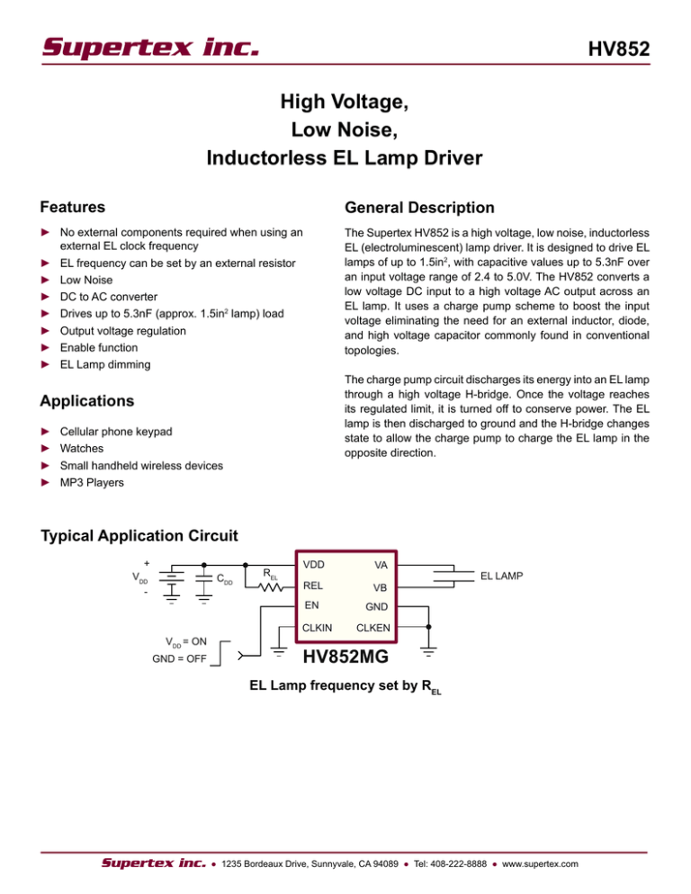
Typical Application Circuit
+
VDD
-
CDD
REL
VDD
VA
REL
VB
EN
VDD = ON
GND = OFF
CLKIN
EL LAMP
GND
CLKEN
HV852MG
EL Lamp frequency set by REL
● 1235 Bordeaux Drive, Sunnyvale, CA 94089 ● Tel: 408-222-8888 ● www.supertex.com
HV852
Pin Configurations
Ordering Information
Package Options
Device
HV852
8-Lead MSOP
10-Lead DFN
3.00x3.00mm body
1.10mm height (max)
0.65mm pitch
3.00x3.00mm body
0.80mm height (max)
0.50mm pitch
HV852MG-G
VDD 1
8 VA
REL 2
7 VB
EN 3
10
2
9
VB
EN
3
8
GND
CLKIN
4
7
GND
VDD 5
6
CLKEN
5 CLKEN
CLKIN 4
HV852K7-G
GND
6
VDD 1
REL
8-Lead MSOP
-G indicates package is RoHS compliant (‘Green’)
VA
10-Lead DFN
(top view)
(top view)
Note:
Pads are at the bottom of the package. Center heat slug is at ground
potential.
Product Marking
Top Marking
Absolute Maximum Ratings
Parameter
H852
LLLL
Value
VDD, supply voltage
-0.5V to 6.5V
Operating temperature
Bottom Marking
-25°C to +85°C
Storage temperature
YYWW
-65°C to +150°C
Power dissipation: 8-Lead MSOP
300mW
Power dissipation: 10-Lead DFN
L = Lot Number
YY = Year Sealed
WW = Week Sealed
= “Green” Packaging
Package may or may not include the following marks: Si or
1.6W
8-Lead MSOP (MG)
Absolute Maximum Ratings are those values beyond which damage to the
device may occur. Functional operation under these conditions is not implied.
Continuous operation of the device at the absolute rating level may affect
device reliability. All voltages are referenced to device ground.
Y = Last Digit of Year Sealed
W = Code for Week Sealed
L = Lot Number
= “Green” Packaging
H852
YWLL
Package may or may not include the following marks: Si or
10-Lead DFN (K7)
Recommended Operating Conditions
Sym
Parameter
Min
Typ
Max
Units
VDD
Input voltage
2.4
-
5.0
V
---
fEL
EL lamp frequency
50
-
500
Hz
---
EL lamp capacitance
0
-
5.3
nF
---
-25
-
+85
°C
---
Cload
TA
Operating temperature
Conditions
● 1235 Bordeaux Drive, Sunnyvale, CA 94089 ● Tel: 408-222-8888 ● www.supertex.com
2
HV852
Electrical Characteristics (Over recommended operating conditions unless otherwise specified:
Sym
Parameter
IDDQ
Quiescent current
TA = 25ºC, VDD = 3.5V)
Min
Typ
Max
Units
-
-
200
nA
Peak output voltage
72
82
92
V
Peak to peak output voltage
144
164
184
V
-
15.2
30
mA
Peak output voltage
72
82
92
V
Peak to peak output voltage
144
164
184
V
fEL
EL lamp frequency
210
250
300
Hz
trout
Output voltage rise time
-
640
-
µs
Min
Typ
Max
Units
0
-
0.5
V
---
1.75
-
VDD
V
VDD = 2.4 to 4.3V. TA = -25 to 85OC
2.0
-
VDD
V
4.3 < VDD ≤ 5.0V. TA = -25 to 85OC
VA or VB
VA-VB
IDD
Operating current
VA or VB
VA-VB
Conditions
EN = 0V
No load
See Figure 1, VDD = 3.5V,
REL = 1.5MΩ, Load = 3.3nF+1kΩ
1.0in2 lamp, 10 to 90% of final value
Logic Inputs
Sym
Parameter
Conditions
VIL
Input logic low voltage
VIH
Input logic high voltage
IIL
Input logic low current
-
-
1.0
µA
VIL = 0V, VDD = 2.4 - 5.0V
IIH
Input logic high current
-
-
1.0
µA
VIH = VDD = 2.4 - 5.0V
trEN
Enable input rise time (for delay turn on)
0.01
-
10
ms
tfEN
Enable input fall time (for delay turn off)
10µ
-
5.0
s
Using external R-C circuit,
see Figure 2
Cin
Logic input capacitance
-
-
10
pF
---
Typical Output Waveform (refer to Figure 1)
Test Conditions:
HV852 driving a 1.0in2 EL lamp
VDD= 3.6V and REL= 1.5MΩ,
VA-VB waveform
● 1235 Bordeaux Drive, Sunnyvale, CA 94089 ● Tel: 408-222-8888 ● www.supertex.com
3
HV852
Functional Block Diagram
VDD
VDD
Capacitor
Charge
Pump Circuit
EN
VA
VSENSE
Feedback
CLKIN
VDD
CLKEN
EL
Oscillator
High
Voltage
Level
Translators
VB
MOSFET
Full Bridge
REL
GND
Typical Performance
(The following was the observed performance when driving a 1.0in2 green lamp)
REL
Load
VDD
(MΩ)
3.3nF+1kΩ
1.5
(V)
(mA)
IDD
VA-VB
2.4
17.56
154
3.0
17.53
158
3.6
17.44
158
4.2
17.65
158
5.0
18.35
158
(V)
Figure 1: Typical Application
+
VDD
REL
CDD
-
VDD
VA
REL
VB
EN
VDD = ON
GND = OFF
EL Lamp
GND
CLKEN
CLKIN
HV852MG
Note:
CDD = 2.2µF, 6.3V ceramic capacitor
Figure 2: Push Button Turn on with Delay Turn off
Push
Button
Turn On
+
VDD
-
REL
VDD
VA
REL
VB
GND
EN
CDD
C
R
EL
Lamp
CLKIN
CLKEN
HV852MG
RC time constant
will set Turn OFF
Delay time
● 1235 Bordeaux Drive, Sunnyvale, CA 94089 ● Tel: 408-222-8888 ● www.supertex.com
4
fEL
(Hz)
245
HV852
Figure 3: Independent Programmable Output Frequency (fEL)
+
VDD
-
CDD
VDD = ON
GND = OFF
VDD
VDD
VA
REL
VB
EN
GND
CLKEN
CLKIN
GND
EL
Lamp
VDD
HV852MG
fCLK
EL Lamp frequency set by an external clock
Note:
fEL = fCLK/128
EL Lamp Dimming Using PWM
EL lamp dimming can be achieved by applying a PWM signal to the ENABLE pin. EL Lamp brightness is proportional to
the PWM signal duty cycle. This is done by pulse skipping the output pulses. The PWM frequency should be kept below
the EL frequency but above 50Hz to avoid flickering.
Figure 4: PWM Dimming Circuit
+
VDD
PWM
Signal
CDD
REL
VDD
GND
2 REL
VB 7
4 CLKIN
EL Lamp
GND 6
CLKEN
5
HV852MG
Name
8-Lead
MSOP
10-Lead
DFN
VDD
1
1, 5
2
VA 8
3 EN
Pin Description
REL
1 VDD
2
Description
Input supply voltage pin.
An external resistor to VDD will set the EL lamp frequency. The EL frequency is inversely
proportional to the REL resistor value. A 1.5MΩ resistor would provide a nominal lamp
frequency of 250Hz.
(1.5MΩ) (250Hz)
fEL =
REL
When using an external clock to set the EL lamp frequency, the REL pin should be
connected to ground.
Enable input pin. Logic high will turn the device on. An external R-C circuit can be added
for a delayed turn off.
Logic input pin. An external logic clock applied to this pin can be used to set the EL lamp
frequency (see Figure 3). The EL lamp frequency is the external clock frequency divided
by 128. This is useful for applications requiring the EL lamp to be synchronized to a
system clock. Connect to ground when not in use.
Logic input pin. Logic high will cause the EL lamp frequency to be set by the CLKIN
input. Logic low will cause the EL lamp frequency to be set by the external REL resistor.
EN
3
3
CLKIN
4
4
CLKEN
5
6
GND
6
7, 8
VB
7
9
EL lamp driver output pin. The EL lamp is connected across VA and VB terminals.
VA
8
10
EL lamp driver output pin. The EL lamp is connected across VA and VB terminals.
IC ground pin.
● 1235 Bordeaux Drive, Sunnyvale, CA 94089 ● Tel: 408-222-8888 ● www.supertex.com
5
HV852
10-Lead DFN Package Outline (K7)
3.00x3.00mm body, 0.80mm height (max), 0.50mm pitch
D
10
D2
10
E
E2
Note 1
(Index Area
D/2 x E/2)
1
e
b
Top View
Note 1
(Index Area
D/2 x E/2)
1
View B
Bottom View
Note 3
θ
A
L
Seating
Plane
A3
L1
Note 2
A1
View B
Side View
Notes:
1. A Pin 1 identifier must be located in the index area indicated. The Pin 1 identifier can be: a molded mark/identifier; an embedded metal marker; or
a printed indicator.
2. Depending on the method of manufacturing, a maximum of 0.15mm pullback (L1) may be present.
3. The inner tip of the lead may be either rounded or square.
Symbol
Dimension
(mm)
A
A1
MIN
0.70
0.00
NOM
0.75
0.02
MAX
0.80
0.05
A3
0.20
REF
b
D
D2
E
E2
0.18
2.85*
2.20
2.85*
1.40
0.25
3.00
-
3.00
-
0.30
3.15*
2.70
3.15*
1.75
e
0.50
BSC
L
L1
θ
0.30
0.00*
0O
0.40
-
-
0.50
0.15
14O
JEDEC Registration MO-229, Variation WEED-5, Issue C, Aug. 2003.
* This dimension is not specified in the JEDEC drawing.
Drawings not to scale.
Supertex Doc.#: DSPD-10DFNK73X3P050, Version D041309.
● 1235 Bordeaux Drive, Sunnyvale, CA 94089 ● Tel: 408-222-8888 ● www.supertex.com
6
HV852
8-Lead MSOP Package Outline (MG)
3.00x3.00mm body, 1.10mm height (max), 0.65mm pitch
D
θ1 (x4)
8
E
E1
Gauge
Plane
L2
Note 1
(Index Area
D/2 x E1/2)
L
1
L1
Top View
A
Seating
Plane
θ
View B
View B
A A2
b
e
A1
Seating
Plane
View A-A
Side View
A
Note:
1. A Pin 1 identifier must be located in the index area indicated. The Pin 1 identifier can be: a molded mark/identifier; an embedded metal marker; or
a printed indicator.
Symbol
Dimension
(mm)
A
A1
A2
b
D
E
E1
MIN
0.75*
0.00
0.75
0.22
2.80*
4.65*
2.80*
NOM
-
-
0.85
-
3.00
4.90
3.00
MAX
1.10
0.15
0.95
0.38
3.20*
5.15*
3.20*
e
0.65
BSC
L
0.40
0.60
0.80
L1
0.95
REF
L2
0.25
BSC
θ
θ1
0
5O
O
-
-
8
15O
O
JEDEC Registration MO-187, Variation AA, Issue E, Dec. 2004.
* This dimension is not specified in the JEDEC drawing.
Drawings are not to scale.
Supertex Doc. #: DSPD-8MSOPMG, Version H041309.
(The package drawing(s) in this data sheet may not reflect the most current specifications. For the latest package outline
information go to http://www.supertex.com/packaging.html.)
Supertex inc. does not recommend the use of its products in life support applications, and will not knowingly sell them for use in such applications unless it receives an
adequate “product liability indemnification insurance agreement.” Supertex inc. does not assume responsibility for use of devices described, and limits its liability to the
replacement of the devices determined defective due to workmanship. No responsibility is assumed for possible omissions and inaccuracies. Circuitry and specifications
are subject to change without notice. For the latest product specifications refer to the Supertex inc. website: http//www.supertex.com.
©2009
All rights reserved. Unauthorized use or reproduction is prohibited.
Doc.# DSFP-HV852
A102309
7
1235 Bordeaux Drive, Sunnyvale, CA 94089
Tel: 408-222-8888
www.supertex.com
