FXO Evaluation Board
Technical Brief TN-101
INTEGRATED CIRCUITS DIVISION
Features
Description
• Provides best-in-class FXO evaluation platform for
PBX/telephony gateway systems with fully
programmable two-wire impedance capability
• A complete, integrated board-level solution that
easily demonstrates FXO and mini-PBX functions
• Uses Le58LQ063 four-channel QLSLAC™ voice
codec/filter from Legerity
• Uses silicon Phone Line Interface (PLI) device
(CPC5620 LITELINK™ III) from IXYS IC Division to
replace bulky transformers and discrete devices to
achieve PC board density
• Legerity-IXYS IC Division voice IC evaluation
platform features a QLSLAC motherboard, PLI
daughtercards and application development
software
• QLSLAC motherboard accommodates four PLI
socket daughtercards for various markets and
applications
• Design to be supported by the Legerity
VoicePath™ script software
• PLI daughtercards provide:
• Two-wire to four-wire hybrid function, isolation,
AC and DC termination
• Loop Start (LS) operation; future boards will
offer Ground Start (GS) operation
• Pulse dial operation in LS or GS modes
• Regulatory surge protection networks
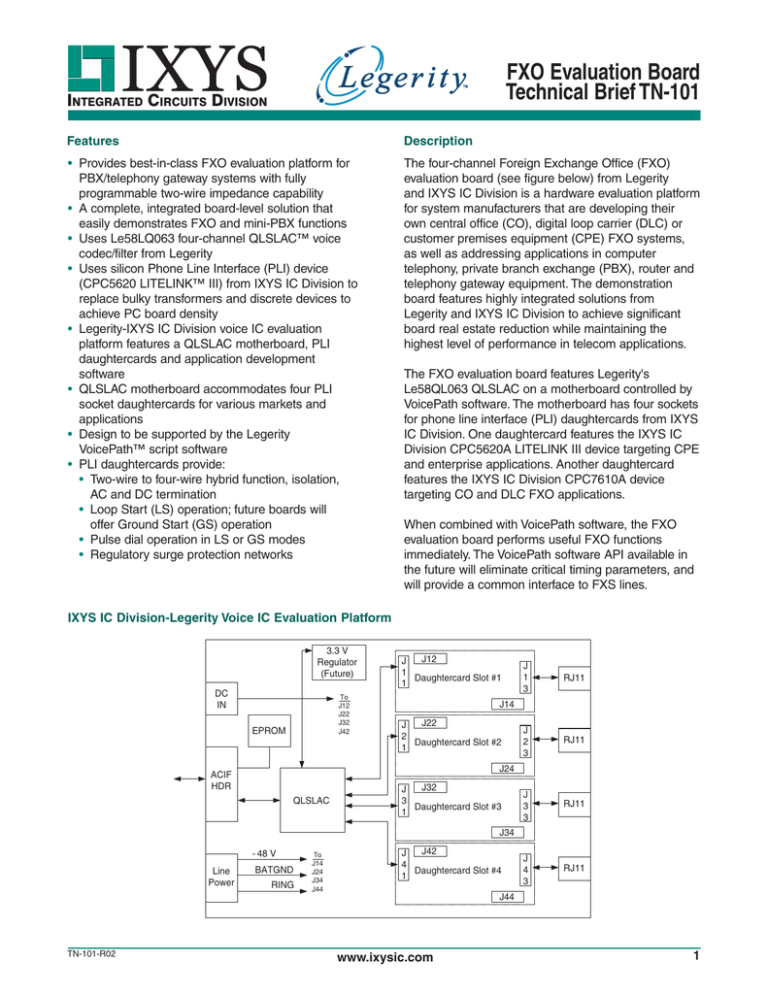
The four-channel Foreign Exchange Office (FXO)
evaluation board (see figure below) from Legerity
and IXYS IC Division is a hardware evaluation platform
for system manufacturers that are developing their
own central office (CO), digital loop carrier (DLC) or
customer premises equipment (CPE) FXO systems,
as well as addressing applications in computer
telephony, private branch exchange (PBX), router and
telephony gateway equipment. The demonstration
board features highly integrated solutions from
Legerity and IXYS IC Division to achieve significant
board real estate reduction while maintaining the
highest level of performance in telecom applications.
The FXO evaluation board features Legerity's
Le58QL063 QLSLAC on a motherboard controlled by
VoicePath software. The motherboard has four sockets
for phone line interface (PLI) daughtercards from IXYS
IC Division. One daughtercard features the IXYS IC
Division CPC5620A LITELINK III device targeting CPE
and enterprise applications. Another daughtercard
features the IXYS IC Division CPC7610A device
targeting CO and DLC FXO applications.
When combined with VoicePath software, the FXO
evaluation board performs useful FXO functions
immediately. The VoicePath software API available in
the future will eliminate critical timing parameters, and
will provide a common interface to FXS lines.
IXYS IC Division-Legerity Voice IC Evaluation Platform
3.3 V
Regulator
(Future)
DC
IN
To
J12
J22
J32
J42
EPROM
J12
J
1
Daughtercard Slot #1
1
J
1
3
RJ11
J
2
3
RJ11
J
3
3
RJ11
J
4
3
RJ11
J14
J22
J
2
Daughtercard Slot #2
1
J24
ACIF
HDR
QLSLAC
J32
J
3
Daughtercard Slot #3
1
J34
- 48 V
Line
Power
BATGND
RING
To
J14
J24
J34
J44
J42
J
4
Daughtercard Slot #4
1
J44
TN-101-R02
www.ixysic.com
1
FXO Evaluation Board
Technical Brief TN-101
INTEGRATED CIRCUITS DIVISION
The VoicePath software and the FXO evaluation board enable customers to reduce their product design cycle time,
and quickly take their products to market. The motherboard provides a test platform to fully test and evaluate the
Legerity QLSLAC device, as well as the PLI daughtercard. A 50-pin telecom connector on the motherboard provides
easy communication and control with the Legerity demonstration and evaluation platforms using an external PC.
The Le58QL063 QLSLAC device is designed to operate in the PCM/MPI mode or in the General Control Interface
(GCI) mode. Demonstration software uses only the PCM/MPI mode of operation, but the design is not limited to MPI
control.
Figure 1. QLSLAC Transmission Block Diagram
Cutoff
Transmit
Path
(CTP)
Digital
TSA
TX
High Pass Filter (HPF)
V IN
*
AX
GIN
ADC
Decimator
Decimator
+
GX
X
*
*
LPF &
HPF
Compressor
TSA Loopback
(TLB)
AISN
Full
Digital
Loopback
(FDL)
*
B
*
*
Cutoff Receive
Path (CRP)
+
V OUT
Z
*
AR
DAC
Interpolator
+
Interpolator
VREF
GR
*
R
Expander
LPF
* Receive
Lower
Gain (LRG)
0
TSA
Digital
RX
1 kHz Tone
(TON)
* programmable blocks
Le58QL063 Device Circuit Description
The QLSLAC device includes the codec and filter functions for each channel. These functions are associated with
the four-wire section of the subscriber line circuitry in a digital switch. The codec converts an analog voice signal
into digital samples and converts digital samples back into an analog signal. During conversion, digital filters are
used to band-limit the voice signals, set the receive and transmit gain, and provide frequency attenuation adjustment
(equalization) of the receive and transmit paths. Transhybrid balancing is also included. Most of the digital filters are
programmable; i.e., their architecture is fixed, but their coefficients can be downloaded from a microprocessor.
The CPC5620 device provides a base two-wire impedance (ZSL). The QLSLAC device uses the AISN and Z-Filter
to modify the base two-wire impedance. This permits one hardware design to address various world market
requirements. The QLSLAC’s B-Filter sections permit the four-wire hybrid balance impedance to be modified to
address most of the world market requirements with no hardware changes. The Ax, Gx, Ar, and Gr sections are used
respectively to control transmission levels for the transmit and receive directions. The R-Filter and the X-Filter can be
used to equalize the frequency response when using complex impedances for the two-wire port.
WinSLAC™ software, which computes all programmable filter coefficients, DC Feed data and supervision data,
accompanies the evaluation board. It allows the designer to enter a description of system requirements. The
WinSLAC software then returns the necessary data and plots the predicted system results. This software is provided
free of charge, and runs on an IBM compatible PC.
The QLSLAC device selectively interfaces with three types of backplanes: Standard PCM/MPI, Standard GCI, and
Modified GCI with a single analog line per GCI channel. A higher level microprocessor can read the line conditions,
and control the line through the MPI or GCI interface. The PCM codes can be either 14-bit linear two's-complement
or 8-bit companded A-law or µ-law.
2
www.ixysic.com
R02
FXO Evaluation Board
Technical Brief TN-101
INTEGRATED CIRCUITS DIVISION
In this design, the QLSLAC device provides adjustable gain, timeslot switching, and frequency response equalization
when using complex impedances. The QLSLAC device can be programmed through the design’s serial MPI interface
to modify the two-wire port impedance and the four-wire balance impedance. The Le58QL063 QLSLAC device can
be operated as a GCI or IOM2 device, and it provides programmable I/O accessible from the MPI interface. These
I/O are used to control the on/off-hook control, detect ringing, detect Tip open, detect loop current, and control ring
ground.
VoicePath software is part of a new generation of product demonstration and evaluation tools for Legerity's voice
interface products. The VoicePath software's graphical user interface (GUI) provides interactive control of all the
programmable features of the QLSLAC device via VPScript. The VPScript software also controls the VoicePath
demonstration board that generates all the digital signals required to operate the SLAC device. In addition to
providing interactive control through the GUI, the VPScript software provides a command language based on the
easy-to-learn and use Tool Command Language (Tcl). Developers can automate more complex control and testing
scenarios by writing Tcl scripts that take full advantage of the programming constructs of Tcl and Legerity’s language
extensions. Currently, scripts are available that demonstrate some of the advanced capabilities of the devices.
Figure 2. CPC5620 Phone Line Interface (PLI) Circuit
TIP+
Isolation Barrier
Tx+
Tx-
Transmit
Diff.
Amplifier
Transmit
Isolation
Amplifier
Transconductance
Stage
2-4 Hybrid
AC/DC Termination
Hook switch
MODE
OH
Vref
AGC
RING
VI Slope Control
AC Impedance Control
Current Limit Control
RING-
Vref
AGC
CID
Receive
Isolation
Amplifier
Rx+
Rx-
Receive
Diff.
Amplifier
CID/
RING
MUX
Snoop Amplifier
CSNOOP
RSNOOP
CSNOOP
RSNOOP
CPC5620 Phone Line Interface (PLI) Circuit Description
The CPC5620 LITELINK III is a single-package optical phone line interface device that targets customer premises
equipment or enterprise applications. The PLI offers a broad feature set, including high-voltage isolation, proper AC
and DC phone line terminations, two-wire to four-wire hybrid function, on-hook and off-hook detection, caller ID, and
half wave ring detect circuitry. Both devices feature a 1500Vrms isolation barrier between the line side and modem
side integrated circuits (ICs) located inside the small 32-pin SOIC package. This eliminates the need for external
optocouplers, transformers or high-voltage capacitors in the data path. The tiny .30" x .38" x .08" package contains
two optically isolated data transmission paths between the line side and modem side circuits. IXYS IC Division’s long
history and expertise in optical coupling have enabled the innovative design and advanced manufacturing of this PLI.
These devices replace bulky magnetic transformers and various other discrete components, and the devices enable
minimized board space, reduced product costs and a simplified manufacturing process in telephony applications.
IXYS IC Division’s LITELINK III has been successfully tested to UL1950, UL1459, UL1577, EN60950, FCC Part 68
and Part 15, and TBR-21.
R02
www.ixysic.com
3
FXO Evaluation Board
Technical Brief TN-101
INTEGRATED CIRCUITS DIVISION
Figure 3. FXO Daughtercard
J2
J
1
+5Vdc, Gnd
TX+
_RING
_CID
CPC5620
CPC7610
Discretes &
Bridge
Protection
Circuit
J
3
_OH
RX+
*GROUND START AND LOOP START CAPABLE
The CPC5620 LITELINK III daughtercard (figure 3) consists of a 32-pin SOIC, a diode bridge, a small FET, and a
few discrete components. The PLI circuitry provides the important loop hold function, ringing detect function, isolation
function, separation of the AC signal from the DC signaling, and the loop signaling function. A "snoop circuit" is
included to permit "on-hook" reception of information, such as caller ID and ring detect.
The CPC5620 device provides sufficient gain/loss in the AC path providing correct transmission levels to the Legerity
QLSLAC device. The CPC5620 is hardware configured to create a two-wire port impedance, which can be modified
to suit nearly any country’s requirements. The CPC5620, combined with the Legerity QLSLAC device, enables a
single design to address the transmission requirements of virtually any country from one hardware design.
IXYS IC Division’s circuitry surrounding the CPC5620 interfaces the loop and ground start signaling to the QLSLAC
device's programmable I/O. The PLI device and its circuitry provide the isolation boundary required by many
countries for both the transmission path and the signaling path. The 1500Vrms isolation protects the line circuit when
used with the suggested surge protection in the design. The CPC5620 LITELINK III design passes the UL1950
safety specification for CPE applications.
4
www.ixysic.com
R02
FXO Evaluation Board
Technical Brief TN-101
INTEGRATED CIRCUITS DIVISION
PERFORMANCE CHARACTERISTICS
Loop Start
Loop Start means that the origination of an outward call occurs with the closure of the DC feed loop drawing feed
current. The serving line circuit provides dial tone based on this seizure. The FXO interface configured for Loop Start
operation floats with respect to ground. The design has surge protection clamps, line-to-line, so that the small signal
audio path is floating. The FXO interface has a very high longitudinal balance, and thus can tolerate large longitudinal
signals. The interface has several potential states:
•
•
•
•
•
Idle drawing no loop current
Off-Hook Transmission (OHT) used for caller ID drawing no loop current
Ringing detection during the active part of ringing cadence
Off-Hook drawing DC loop current, and providing an AC termination to the loop
Dial pulse state drawing DC current as a pure resistance (for low pulse distortion)
The ringing detector detects ringing signals greater than 40Vrms as ringing, while presenting less than one REN AC
load. The loop hold circuit, which draws the DC current during the "off-hook" state, bridges the AC termination, and
has a high enough impedance at voice frequencies that it does not effect the AC termination value or transmission
levels.
Ground Start
Ground Start is a more complex signaling protocol primarily used for two-way calls. This protocol reduces the
"glare" period where both the serving line and the FXO line are trying to initiate a call at the same time. The Ground
Start protocol requires the serving line circuit to idle with the TIP lead OPEN (i.e. a high resistance to ground). The
request for service from the FXO interface is the application of a low resistance to ground on the RING lead. When
the serving line detects the ring ground current flow, the serving line connects the TIP lead with a low resistance to
ground. The potential must be nearly zero volts and be able to sink several mA. of current. The FXO replies to the Tip
ground at the serving line by removing the Ring Ground and simultaneously applying a loop condition. The FXO is
now "off-hook" and active. The FXO expects to begin address signaling (receiving dial tone).
During an inward call (into the FXO), the serving line applies the ringing alerting signal simultaneously connecting
the TIP lead via a low resistance path to ground. During the silent interval of ringing, the serving line holds the TIP
lead at a "near ground" potential and battery on the RING lead. The FXO answers the call either during the alerting
period or during the silent interval by a loop closure.
FXO General Operation
The loop hold function must draw greater than 18 mA with less than 8 Volts across Tip and Ring. It must not
overheat on a short or low-resistance loop where the full battery is pushing loop current. The loop hold function must
provide a high AC impedance bridging the loop so that the loop hold does not load the transmission path or modify
the AC 2W termination impedance. Nearly all the loop hold circuits are either constant-current sinks or gyrators
(synthesized inductance). These implementations are not compatible with dial pulsing as they cause significant dial
pulse distortion. The loop hold circuit is modified during dial-pulse signaling to reduce the dial-pulse distortion. The
constant-current loop hold circuits must not be too ideal. The compliance or equivalent shunt resistance of the current
sink must be low enough to permit the serving line to use a constant current feed. Poor choice of constant-current
loop hold circuit parameters cause either oscillation between SLIC and loop hold, saturation of the SLIC device or
saturation of the loop hold. The IXYS IC Division PLI in this design uses a gyrator-based design, eliminating these
problems.
The requirement for Ground Start signaling can be thought of as a signaling appliqué circuit. While the lightning
protection for Ground Start as an applique (add-on) is slightly more expensive than an integrated solution, the
R02
www.ixysic.com
5
INTEGRATED CIRCUITS DIVISION
FXO Evaluation Board
Technical Brief TN-101
presented design permits easy removal of the Ground Start added cost. All FXO interfaces require the Loop Start
signaling. Those cases not requiring the Ground Start option can delete that circuitry for a cost savings. Most
customers need Ground Start as an option.
Nearly all FXO interfaces in North America operate at 0 dBr or -2 dBr in the direction of transmission toward the
two-wire port (Legerity's receive direction). North America prefers the two-wire to four-wire direction (Legerity's
transmit direction) to be typically 0 dBr to preserve the signal-to-noise ratio while the signal is carried by the digital
means. In other world markets, there are situations where the receive relative level may be as high as +0 dBr. The
transmit or two-wire to four-wire direction may also have gain. This places a burden on the FXO interface of dealing
with higher than normal signal levels. The programmable gain setting of the Legerity QLSLAC device enables country
specific settings handled by the system software. Legerity’s VoicePath software enables on-the-fly gain changes as
required.
Impedances
The reference design and the associated software provide three two-wire port impedances and three four-wire
balance impedances. The Legerity WinSLAC software also enables the designer to add impedances or other
transmission changes with the seamless tool chain provided in the VoicePath software. The Legerity VoicePath
software and the associated VPWizard (part of the SDK) permit the designer to incorporate, quickly and easily, any
number of other impedances.
Voltage/Current Templates (V/I)
The IXYS IC Division DAA can provide more than one V/I characteristic. This characteristic is set by a resistor in
the design. IXYS IC Division produces several methods of including this selection of different V/I template, and has
application information showing how the daughtercard can include this feature.
Support
The FXO evaluation platform is supported by field application engineers (FAEs) from both IXYS IC Division and
Legerity. IXYS IC Division FAEs will address questions that concern the DAA portion of the evaluation board, and
Legerity FAEs will address queries dealing with QLSLAC device functions. Both companies are eager to assist
customers in understanding and applying this best-in-class FXO evaluation platform to their system design needs.
FXO Terminology
Foreign Exchange Office (FXO) is a service that can be ordered from a telco that provides local phone services
from a CO that is outside (foreign to) the subscriber’s exchange area. In its simplest form, a subscriber can pick up
the phone in one city and receive a dial tone in the "foreign" city. This type of connection is provided by FX trunks.
FX trunk signaling can be provided over analog or T1 links. Connecting POTS telephones to a computer telephony
system via T1 links requires a channel bank configured with FX-type connections. Generating a call from a POTS
phone to a computer telephony system or a PBX system requires configuration of an FXO connection. The volume
of requests for this type of service is increasing as new service providers enter the market and bypass the traditional
telephone network.
For additional information please visit our website at: www.ixysic.com
IXYS Integrated Circuits Division makes no representations or warranties with respect to the accuracy or completeness of the contents of this publication and reserves the right to make
changes to specifications and product descriptions at any time without notice. Neither circuit patent licenses nor indemnity are expressed or implied. Except as set forth in IXYS Integrated
Circuits Division’s Standard Terms and Conditions of Sale, IXYS Integrated Circuits Division assumes no liability whatsoever, and disclaims any express or implied warranty, relating to its
products including, but not limited to, the implied warranty of merchantability, fitness for a particular purpose, or infringement of any intellectual property right.
The products described in this document are not designed, intended, authorized or warranted for use as components in systems intended for surgical implant into the body, or in other
applications intended to support or sustain life, or where malfunction of IXYS Integrated Circuits Division’s product may result in direct physical harm, injury, or death to a person or severe
property or environmental damage. IXYS Integrated Circuits Division reserves the right to discontinue or make changes to its products at any time without notice.
6
Specification: TN-101-R02
©Copyright 2014, IXYS Integrated Circuits Division
All rights reserved. Printed in USA.
10/7/2014


