Freescale Semiconductor
Engineering Bulletin
EB213
Rev. 0, 5/2003
Surge - Ringing Wave Clamp for GaAs
CATV Module Protection
by: Jeff Gengler
Freescale Semiconductor
INTRODUCTION
CLAMP DEVICE SELECTION CRITERIA
CATV amplifiers are required to withstand surges induced
by nearby lightning strikes. Manufactures use crowbar
devices such as gas discharge tubes and semiconductor
devices that are intended to limit surge voltages and conduct
surge currents. These devices have a very fast turn - on once
their threshold voltage is reached, causing a very fast change
in voltages (dv/dt). This in turn induces several cycles of high
voltage ringing within the pass band of the diplex filter,
allowing the surge- ringing wave to propagate to the output of
the hybrid module. Commonly deployed crowbar devices
such as gas discharge tubes generate a few cycles as high as
200 V peaks at 50 to 150 MHz when they fire during a 6 kV
surge event. Because GaAs CATV modules are susceptible
to ring wave stresses, a surge- ringing wave clamp is needed
for additional protection.
The surge - ringing wave clamp is constructed using two
silicon bipolar transistors. The bipolar transistor device
chosen is critical for successful surge ring wave clamping.
Commercially available RF bipolar transistors are suitable
devices because the surge - ringing waves are within the
CATV pass band. The criteria for a clamp device is as follows:
1. The transistor should have a transition frequency with a
minimum of 5 GHz to ensure sufficient reaction speed to
incoming surge - ringing waves.
2. The collector - to - emitter breakdown voltage (V(BR)CEO)
of each individual transistor should have a high enough
breakdown voltage to avoid impacting distortion
performance. If this parameter is too low, the high output
voltage peaks will be clipped, causing degradation in
distortion performance. The V(BR)CEO should be selected
SURGE- RINGING WAVE CLAMP
above the peak output but not too far above the peak
voltage output. The most effective clamp has the lowest
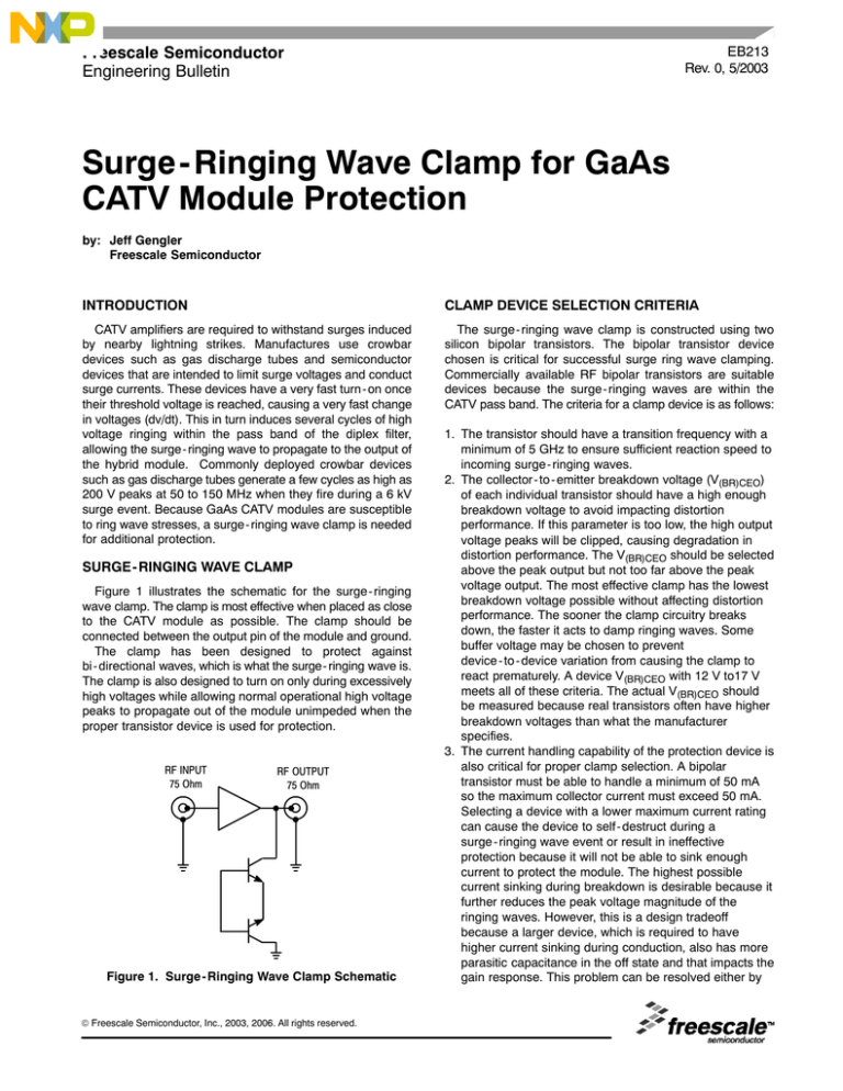
Figure 1 illustrates the schematic for the surge - ringing
breakdown voltage possible without affecting distortion
wave clamp. The clamp is most effective when placed as close
performance. The sooner the clamp circuitry breaks
to the CATV module as possible. The clamp should be
down, the faster it acts to damp ringing waves. Some
connected between the output pin of the module and ground.
buffer voltage may be chosen to prevent
The clamp has been designed to protect against
device - to - device variation from causing the clamp to
bi - directional waves, which is what the surge- ringing wave is.
react prematurely. A device V(BR)CEO with 12 V to17 V
The clamp is also designed to turn on only during excessively
meets all of these criteria. The actual V(BR)CEO should
high voltages while allowing normal operational high voltage
be measured because real transistors often have higher
peaks to propagate out of the module unimpeded when the
breakdown voltages than what the manufacturer
proper transistor device is used for protection.
specifies.
3. The current handling capability of the protection device is
also critical for proper clamp selection. A bipolar
RF INPUT
RF OUTPUT
transistor must be able to handle a minimum of 50 mA
75 Ohm
75 Ohm
so the maximum collector current must exceed 50 mA.
Selecting a device with a lower maximum current rating
can cause the device to self - destruct during a
surge - ringing wave event or result in ineffective
protection because it will not be able to sink enough
current to protect the module. The highest possible
current sinking during breakdown is desirable because it
further reduces the peak voltage magnitude of the
ringing waves. However, this is a design tradeoff
because a larger device, which is required to have
higher current sinking during conduction, also has more
parasitic capacitance in the off state and that impacts the
Figure 1. Surge - Ringing Wave Clamp Schematic
gain response. This problem can be resolved either by
designing around it or selecting a device that
compromises the amount of current it can sink (as long
© Freescale Semiconductor, Inc., 2003, 2006. All rights reserved.
EB213
RF Engineering Bulletin
Freescale Semiconductor
1
as the minimum requirement is met) and the amount of
capacitance the clamp introduces. Devices close to the
minimum often have negligible parasitic capacitance,
and no special response considerations are necessary.
CONCLUSION
To ensure field reliability of GaAs CATV modules, additional
protection circuitry must be implemented. Incorporation of the
ringing wave clamp shown in Figure 1 results in a major
reduction in the voltage magnitude of offending waves during
surge events to a level that will not harm GaAs CATV modules.
Proper bipolar transistor device selection when used in the
surge - ringing wave clamp configuration is an effective means
of protection without impacting distortion performance. A
reduction of more than 80% in the peak voltages of the ringing
waves has been demonstrated in some applications when the
clamp is applied versus those in an unprotected module.
The transistor devices used to realize the clamp protection
circuitry is important. There are many different commercially
available bipolar transistors that meet the criteria to be
implemented in the surge - ringing wave clamp configuration
that the designer can choose from to incorporate packaged
transistors into a design. Bipolar transistors are very
inexpensive so the extra cost of the additional components is
easily offset by the increased field reliability that they provide
against lightning - induced surges.
EB213
2
RF Engineering Bulletin
Freescale Semiconductor
How to Reach Us:
Home Page:
www.freescale.com
E - mail:
support@freescale.com
USA/Europe or Locations Not Listed:
Freescale Semiconductor
Technical Information Center, CH370
1300 N. Alma School Road
Chandler, Arizona 85224
+1 - 800 - 521 - 6274 or +1 - 480 - 768 - 2130
support@freescale.com
Europe, Middle East, and Africa:
Freescale Halbleiter Deutschland GmbH
Technical Information Center
Schatzbogen 7
81829 Muenchen, Germany
+44 1296 380 456 (English)
+46 8 52200080 (English)
+49 89 92103 559 (German)
+33 1 69 35 48 48 (French)
support@freescale.com
Japan:
Freescale Semiconductor Japan Ltd.
Headquarters
ARCO Tower 15F
1 - 8 - 1, Shimo - Meguro, Meguro - ku,
Tokyo 153 - 0064
Japan
0120 191014 or +81 3 5437 9125
support.japan@freescale.com
Asia/Pacific:
Freescale Semiconductor Hong Kong Ltd.
Technical Information Center
2 Dai King Street
Tai Po Industrial Estate
Tai Po, N.T., Hong Kong
+800 2666 8080
support.asia@freescale.com
For Literature Requests Only:
Freescale Semiconductor Literature Distribution Center
P.O. Box 5405
Denver, Colorado 80217
1 - 800 - 441 - 2447 or 303 - 675 - 2140
Fax: 303 - 675 - 2150
LDCForFreescaleSemiconductor@hibbertgroup.com
Information in this document is provided solely to enable system and software
implementers to use Freescale Semiconductor products. There are no express or
implied copyright licenses granted hereunder to design or fabricate any integrated
circuits or integrated circuits based on the information in this document.
Freescale Semiconductor reserves the right to make changes without further notice to
any products herein. Freescale Semiconductor makes no warranty, representation or
guarantee regarding the suitability of its products for any particular purpose, nor does
Freescale Semiconductor assume any liability arising out of the application or use of
any product or circuit, and specifically disclaims any and all liability, including without
limitation consequential or incidental damages. “Typical” parameters that may be
provided in Freescale Semiconductor data sheets and/or specifications can and do
vary in different applications and actual performance may vary over time. All operating
parameters, including “Typicals”, must be validated for each customer application by
customer’s technical experts. Freescale Semiconductor does not convey any license
under its patent rights nor the rights of others. Freescale Semiconductor products are
not designed, intended, or authorized for use as components in systems intended for
surgical implant into the body, or other applications intended to support or sustain life,
or for any other application in which the failure of the Freescale Semiconductor product
could create a situation where personal injury or death may occur. Should Buyer
purchase or use Freescale Semiconductor products for any such unintended or
unauthorized application, Buyer shall indemnify and hold Freescale Semiconductor
and its officers, employees, subsidiaries, affiliates, and distributors harmless against all
claims, costs, damages, and expenses, and reasonable attorney fees arising out of,
directly or indirectly, any claim of personal injury or death associated with such
unintended or unauthorized use, even if such claim alleges that Freescale
Semiconductor was negligent regarding the design or manufacture of the part.
Freescalet and the Freescale logo are trademarks of Freescale Semiconductor, Inc.
All other product or service names are the property of their respective owners.
© Freescale Semiconductor, Inc. 2003, 2006. All rights reserved.
EB213
RF
Engineering Bulletin
EB213
Rev. 0, 5/2003
Freescale
Semiconductor
3
