TS921
RAIL TO RAIL HIGH OUTPUT CURRENT
SINGLE OPERATIONAL AMPLIFIER
..
..
..
..
RAIL TO RAIL INPUT AND OUTPUT
LOW NOISE : 9nV/√
√
(Hz)
)
LOW DISTORTION
HIGH OUTPUT CURRENT : 80mA
(able to drive 32Ω loads)
HIGH SPEED : 4MHz, 1V/µs
OPERATING FROM 2.7V to 12V
ESD INTERNAL PROTECTION : 1.5KV
LATCH-UP IMMUNITY
N
DIP8
(Plastic Package)
D
SO8
(Plastic Micropackage)
ORDER CODES
Part Number
DESCRIPTION
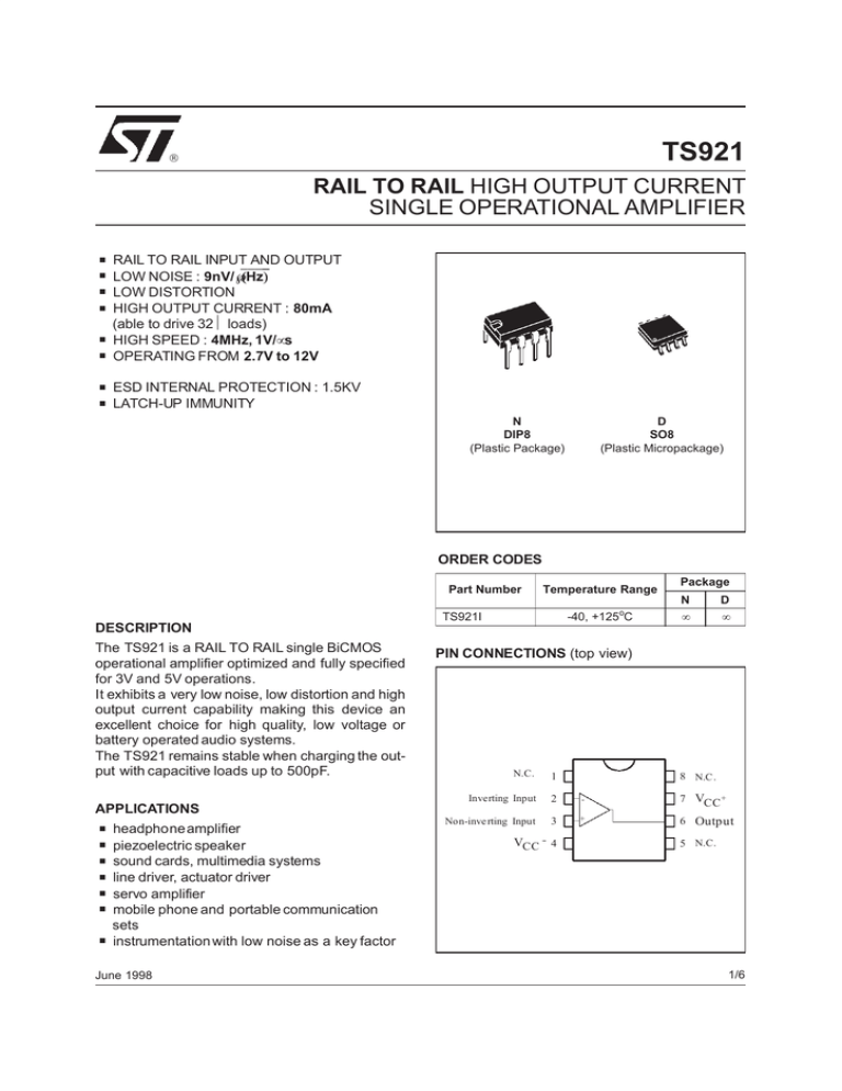
The TS921 is a RAIL TO RAIL single BiCMOS
operational amplifier optimized and fully specified
for 3V and 5V operations.
It exhibits a very low noise, low distortion and high
output current capability making this device an
excellent choice for high quality, low voltage or
battery operated audio systems.
The TS921 remains stable when charging the output with capacitive loads up to 500pF.
..
..
..
.
-40, +125oC
TS921I
June 1998
Package
N
D
•
•
PIN CONNECTIONS (top view)
N.C.
1
Inverting Input
2
-
7 VCC +
Non-inve rting Input
3
+
6 Output
APPLICATIONS
headphoneamplifier
piezoelectric speaker
sound cards, multimedia systems
line driver, actuator driver
servo amplifier
mobile phone and portable communication
sets
instrumentation with low noise as a key factor
Temperature Range
VCC 4
8 N.C.
5 N.C.
1/6
TS921
ABSOLUTE MAXIMUM RATINGS
Symbol
Parameter
Value
Unit
VCC
Supply Voltage - (note 1)
12
V
Vid
Differential Input Voltage - (note 2)
±1
V
Vi
Input Voltage - (note 3)
-0.3 to 14
V
Toper
Operating Free Air Temperature Range
-40 to +125
o
Tstg
Storage Temperature
-65 to +150
o
150
o
see note 4
o
Maximum Junction Temperature
Tj
Output Short Circuit Duration
Notes :
1.
2.
3.
4.
C
C
C
C
All voltage values, except differential voltage are with respect to network ground terminal.
Differential voltages are the non-inverting input terminal with respect to the inverting input terminal.
The magnitude of input and output voltages must never exceed VCC+ +0.3V.
Short-circuits can cause excessive heating.
OPERATING CONDITIONS
Symbol
2/6
Parameter
VCC
Supply Voltage
Vicm
Common Mode Input Voltage Range
Value
Unit
2.7 to 12
V
VCC- -0.2 to VCC++0.2
V
TS921
ELECTRICAL CHARACTERISTICS
VCC+ = 3V, Tamb = 25oC (unless otherwise specified)
Symbol
Vio
DVio
Iio
Iib
VOH
VOL
Parameter
Input Offset Voltage
Tmin. ≤ Tamb ≤ Tmax.
Input Offset Voltage Drift
Input Offset Current
Vout = 1.5V
Input Bias Current
Vout = 1.5V
High Level Output Voltage
Low Level Output Voltage
Avd
Large Signal Voltage Gain (Vout = 2Vpk-pk)
ICC
Supply Current
no load, Vout = VCC/2
Gain Bandwidth Product
GBP
Min.
Io
SR
∅m
Gm
en
THD
Max.
3
5
Unit
mV
µV/oC
nA
2
30
nA
15
RL = 600Ω
R L = 32Ω
R L = 600Ω
R L = 32Ω
R L = 600Ω
R L = 32Ω
100
2.87
V
2.63
100
180
35
16
mV
V/mV
mA
1
1.5
MHz
R L = 600Ω
CMR
SVR
Typ.
Common Mode Rejection Ratio
Supply Voltage Rejection Ratio
VCC = 2.7 to 3.3V
Output Short Circuit Current
Slew Rate
Phase Margin at Unity Gain
RL = 600Ω,CL = 100pF
Gain Margin
RL = 600Ω,CL = 100pF
Equivalent Input Noise Voltage
f = 1kHz
Total Harmonic Distortion
Vout = 2Vpk-pk, F = 1kHz, AV = 1, RL = 600Ω
60
4
80
60
50
0.7
80
80
1
dB
dB
mA
V/µs
Degrees
68
dB
12
9
nV
√
Hz
%
0.005
3/6
TS921
ELECTRICAL CHARACTERISTICS
VCC+ = 5V, Tamb = 25oC (unless otherwise specified)
Symbol
Vio
DVio
Iio
Iib
VOH
VOL
Low Level Output Voltage
Avd
Large Signal Voltage Gain (Vout = 2Vpk-pk)
ICC
Supply Current
no load, Vout = VCC/2
Gain Bandwidth Product
R L = 600Ω
Common Mode Rejection Ratio
Supply Voltage Rejection Ratio
VCC = 2.7 to 3.3V
Output Short Circuit Current
Slew Rate
Phase Margin at Unity Gain
R L = 600Ω,CL = 100pF
Gain Margin
R L = 600Ω,CL = 100pF
GBP
CMR
SVR
Io
SR
∅m
Gm
en
THD
4/6
Parameter
Input Offset Voltage
Tmin. ≤ Tamb ≤ Tmax.
Input Offset Voltage Drift
Input Offset Current
Vout = 1.5V
Input Bias Current
Vout = 1.5V
High Level Output Voltage
Min.
Typ.
Max.
3
5
Unit
mV
µV/oC
nA
2
30
nA
15
RL = 600Ω
RL = 32Ω
RL = 600Ω
RL = 32Ω
RL = 600Ω
RL = 32Ω
Equivalent Input Noise Voltage
f = 1kHz
Total Harmonic Distortion
Vout = 2Vpk-pk, F = 1kHz, AV = 1, R L = 600Ω
100
4.85
V
4.4
120
300
35
16
mV
V/mV
mA
1
1.5
MHz
60
4
80
60
50
0.7
80
80
1
dB
dB
mA
V/µs
Degrees
68
dB
12
9
0.005
nV
√
Hz
%
TS921
PACKAGE MECHANICAL DATA
8 PINS - PLASTIC PACKAGE
Dimensions
A
a1
B
b
b1
D
E
e
e3
e4
F
i
L
Z
Min.
Millimeters
Typ.
3.32
0.51
1.15
0.356
0.204
Max.
1.65
0.55
0.304
10.92
9.75
7.95
Min.
0.020
0.045
0.014
0.008
Max.
0.065
0.022
0.012
0.430
0.384
0.313
2.54
7.62
7.62
3.18
Inches
Typ.
0.131
0.100
0.300
0.300
6.6
5.08
3.81
1.52
0.125
0260
0.200
0.150
0.060
5/6
TS921
PACKAGE MECHANICAL DATA
8 PINS - PLASTIC MICROPACKAGE (SO)
Dimensions
A
a1
a2
a3
b
b1
C
c1
D
E
e
e3
F
L
M
S
Min.
Millimeters
Typ.
0.1
0.65
0.35
0.19
0.25
Max.
1.75
0.25
1.65
0.85
0.48
0.25
0.5
Min.
Inches
Typ.
0.026
0.014
0.007
0.010
Max.
0.069
0.010
0.065
0.033
0.019
0.010
0.020
0.189
0.228
0.197
0.244
0.004
o
45 (typ.)
4.8
5.8
5.0
6.2
1.27
3.81
3.8
0.4
0.050
0.150
4.0
1.27
0.6
0.150
0.016
0.157
0.050
0.024
o
8 (max.)
1998 STMicroelectronics – Printed in Italy – All Rights Reserved
STMicroelectronics GROUP OF COMPANIES
Australia - Brazil - Canada - China - France - Germany - Italy - Japan - Korea - Malaysia - Malta - Mexico - Morocco
The Netherlands - Singapore - Spain - Sweden - Switzerland - Taiwan - Thailand - United Kingdom - U.S.A.
6/6
ORDER CODE :
Information furnished is believed to be accurate and reliable. However, STMicroelectronics assumes no responsibility for the
consequences of use of such information nor for any infringement of patents or other rights of third parties which may result from
its use. No license is granted by implication or otherwise under any patent or patent rights of STMicroelectronics. Specifications
mentioned in this publication are subject to change without notice. This publ ication supersedes and replaces all infor mation
previously supplied. STMicroelectronics products are not authorized for use as critical components in life support devices or systems
without express written approval of STMicroelectronics.
The ST logo is a trademark of STMicroelectronics


