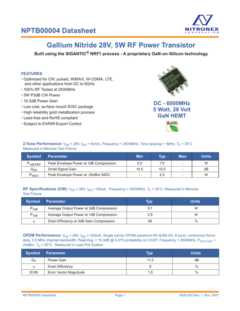
NPTB00004 Datasheet
Gallium Nitride 28V, 5W RF Power Transistor
Built using the SIGANTIC® NRF1 process - A proprietary GaN-on-Silicon technology
FEATURES
• Optimized for CW, pulsed, WiMAX, W-CDMA, LTE,
and other applications from DC to 6GHz
• 100% RF Tested at 2500MHz
• 5W P3dB CW Power
• 15.5dB Power Gain
• Low cost, surface mount SOIC package
• High reliability gold metallization process
• Lead-free and RoHS compliant
• Subject to EAR99 Export Control
DC - 6000MHz
5 Watt, 28 Volt
GaN HEMT
2-Tone Performance: VDS = 28V, IDQ = 50mA, Frequency = 2500MHz, Tone spacing = 1MHz, TC = 25°C
Measured in Nitronex Test Fixture
Symbol
Parameter
Min
Typ
Max
Units
P1dB,PEP
Peak Envelope Power at 1dB Compression
5.0
7.5
-
W
Small Signal Gain
14.5
15.5
-
dB
-
2.5
-
W
GSS
PIMD3
Peak Envelope Power at -35dBm IMD3
RF Specifications (CW): VDS = 28V, IDQ = 50mA, Frequency = 2500MHz, TC = 25°C, Measured in Nitronex
Test Fixture
Symbol
Parameter
Typ
Units
P3dB
Average Output Power at 3dB Compression
5.1
W
P1dB
Average Output Power at 1dB Compression
2.9
W
Drain Efficiency at 3dB Gain Compression
56
%
h
OFDM Performance: VDS = 28V, IDQ = 100mA, Single carrier OFDM waveform 64-QAM 3/4, 8 burst, continuous frame
data, 3.5 MHz channel bandwidth. Peak/Avg. = 10.3dB @ 0.01% probability on CCDF. Frequency = 3500MHz, POUT,AVG =
24dBm, TC = 25°C. Measured in Load Pull System
Symbol
GP
h
EVM
Parameter
Typ
Units
Power Gain
11.2
dB
9
%
1.0
%
Drain Efficiency
Error Vector Magnitude
NPTB00004 Datasheet
Page 1
NDS-002 Rev. 1, Nov. 2007
NPTB00004 Datasheet
DC Specifications: TC=25°C
Symbol
Parameter
Min
Typ
Max
Units
100
-
-
V
-
0.5
2
mA
Off Characteristics
VBDS
IDLK
Drain-Source Breakdown Voltage
(VGS = -8V, ID = 2mA)
Drain-Source Leakage Current
(VGS = -8V, VDS = 60V)
On Characteristics
VT
Gate Threshold Voltage
(VDS = 28V, ID = 2mA)
-2.0
-1.5
-1.0
V
VGSQ
Gate Quiescent Voltage
(VDS = 28V, ID = 50mA)
-1.8
-1.3
-0.8
V
RON
On Resistance
(VGS = 2V, ID = 15mA)
-
2.0
2.2
W
1.1
1.3
-
A
ID
Drain Current
(VDS = 7V pulsed, 300ms pulse width,
0.2% duty cycle, VGS = 2V)
Absolute Maximum Ratings: Not simultaneous, TC=25°C unless otherwise noted
Symbol
Parameter
Max
Units
VDS
Drain-Source Voltage
100
V
VGS
Gate-Source Voltage
-10 to 3
V
7.6
W
PT
Total Device Power Dissipation (Derated above 25°C)
qJC
Thermal Resistance (Junction-to-Case)
TSTG
TJ
Storage Temperature Range
Operating Junction Temperature
23
°C/W
-65 to 150
°C
200
°C
HBM
Human Body Model ESD Rating (per JESD22-A114)
MM
Machine Model ESD Rating (per JESD22-A115)
MSL
Moisture Sensitivity Level (per IPC/JEDEC J-STD-020): Rating of 3 at 260 °C Package Peak Temperature
NPTB00004 Datasheet
Page 2
1A (>250V)
M1(>50V)
NDS-002 Rev. 1, Nov. 2007
NPTB00004 Datasheet
Table 1: Optimum Source and Load Impedances (VDS = 28V)
Frequency
ZS (W)
ZL (W)
IDQ (mA)
Optimized Tuning Condtion
900
9.2 + j23.8
52.6 + j22.8
50
CW Power and Efficiency
1800
5.2 + j0.5
24.5 + j18.3
50
CW Power and Efficiency
2140
5.0 - j2.6
17.1 + j15.0
50
CW Power and Efficiency
2500
5.4 - j10.5
14.7 + j10.0
50
CW Power and Efficiency
3500
5.0 - j21.0
11.2 + j4.7
50
CW Power and Efficiency
900
21.9 + j43.4
59.5 + j33.7
100
W-CDMA, POUT, Efficiency, -45dBc ACPR
1800
13.1 + j24.3
34.5 + j48.8
100
W-CDMA, POUT, Efficiency, -45dBc ACPR
2140
5.4 + j17.3
25.4 + j36.4
100
W-CDMA, POUT, Efficiency, -45dBc ACPR
2600
4.0 + j6.8
12.2 + j25.8
100
LTE, POUT, Efficiency, -45dBc ACPR
2500
5.0 + j16.2
13.2 + j20.4
100
OFDM, Maximum POUT, 1.5% EVM
3500
4.1 - j0.6
6.6 + j10.5
100
OFDM, Maximum POUT, 1.5% EVM
ZS is the source impedance
presented to the device.
ZL is the load impedance
presented to the device.
Figure 1 - Impedances for Optimum CW Power, VDS = 28V, IDQ = 50mA
NPTB00004 Datasheet
Page 3
NDS-002 Rev. 1, Nov. 2007
NPTB00004 Datasheet
Figure 2 - Typical CW Performance in Load-Pull
System, VDS = 28V, IDQ = 50mA,
Frequency = 900MHz
Figure 3 - Typical CW Performance in Load-Pull
System, VDS = 28V, IDQ = 50mA,
Frequency = 2500MHz
Figure 4 - Typical CW Performance in Load-Pull
System, VDS = 28V, IDQ = 50mA,
Frequency = 3500MHz
Figure 5 - Typical CW Performance in Load-Pull
System, VDS = 28V, IDQ = 50mA,
Frequency = 900 to 3500MHz
NPTB00004 Datasheet
Page 4
NDS-002 Rev. 1, Nov. 2007
NPTB00004 Datasheet
Figure 6 - Typical CW Performance in Load-Pull
System Over Ambient Temperature,
VDS = 28V, IDQ = 50mA, Frequency = 2500MHz
Figure 7 - Typical OFDM Performance in Load-Pull
System, VDS = 28V, IDQ = 100mA,
Frequency = 2500MHz
Figure 8 - Typical OFDM Performance in Load-Pull
System, VDS = 28V, IDQ = 100mA,
Frequency = 3500MHz
Figure 9 - Typical W-CDMA Performance in
Load-Pull System, VDS = 28V, IDQ = 100mA,
Frequency = 900MHz
NPTB00004 Datasheet
Page 5
NDS-002 Rev. 1, Nov. 2007
NPTB00004 Datasheet
Figure 10 - Typical W-CDMA Performance in
Load-Pull System, VDS = 28V, IDQ = 100mA,
Frequency = 1800MHz
Figure 11 - Typical W-CDMA Performance in
Load-Pull System, VDS = 28V, IDQ = 100mA,
Frequency = 2140MHz
Figure 13 - Quiescient Gate Voltage (VGSQ) Required
to Reach IDQ = 50mA as a Function of
Ambient Temperature, Measured in Nitronex
Test Fixture, VDS = 28V
Figure 12 - Typical LTE Performance in Load-Pull
System, VDS = 28V, IDQ = 100mA,
Frequency = 2600MHz. Single Carrier OFDM,
64-QAM 3/4, 8 burst, 20 MHz Bandwidth,
Peak/Avg = 9.5dB @ 0.01% probability on CCDF
NPTB00004 Datasheet
Page 6
NDS-002 Rev. 1, Nov. 2007
NPTB00004 Datasheet
Figure 14 - Power Derating Curve
NPTB00004 Datasheet
Figure 15 - MTTF of NRF1 Devices as a
Function of Junction Temperature
Page 7
NDS-002 Rev. 1, Nov. 2007
NPTB00004 Datasheet
Figure 16 - APP-NPTB00004-25 2500MHz Demonstration Board
Figure 17 - APP-NPTB00004-25 2500MHz Demonstration Board Equivalent Circuit
NPTB00004 Datasheet
Page 8
NDS-002 Rev. 1, Nov. 2007
NPTB00004 Datasheet
Table 2: APP-NPTB00004-25 2500MHz Demonstration Board Bill of Materials
Name
Value
Tolerance
Vendor
Vendor Number
C1
10uF
20%
AVX
TAJA106M016R
C2
1uF
10%
AVX
12101C105KAT2A
C3
0.1uF
10%
Murata
GRM188R72A104KA35D
C4
0.01uF
10%
AVX
06031C103KAT2A
10%
AVX
06031C102KAT2A
Panasonic
ECE-V1JA101P
C5
0.001uF
C6, C12
Do Not Place
C7
100uF
20%
C8
1uF
10%
AVX
12101C105KAT2A
C9
0.1uF
10%
Murata
GRM188R72A104KA35D
C10
0.01uF
10%
AVX
06031C103KAT2A
C11
0.001uF
10%
AVX
06031C102KAT2A
C13
2.7pF
+/- 0.1pF
ATC
ATC600F2R7B
C14
10pF
1%
ATC
ATC600F100B
C15
33pF
1%
ATC
ATC600F330B
C16
33pF
1%
ATC
ATC600F330B
CC1, CC3
Do Not Place
R1
200 ohm
1%
Panasonic
ERJ-2GEJ201X
R2, R3, R5
0 ohm
--
Panasonic
ERJ-2GE0R00X
R4
0.033 ohm
1%
Panasonic
ERJ-6BWJR033W
NBD-012_Rev1
--
--
Alberta Printed Circuits
NBD-012_Rev1
Rogers
R04350, t = 30mil er = 3.5
Substrate
NPTB00004 Datasheet
Page 9
NDS-002 Rev. 1, Nov. 2007
NPTB00004 Datasheet
Ordering Information1
Part Number
Description
NPTB00004D
NPTB00004 in D (PSOP2) Package
1: To find a Nitronex contact in your area, visit our website at http://www.nitronex.com
D Package Dimensions and Pinout
Inches
Millimeters
A
Dim
Min
Max
Min
C
A
0.189
0.196
4.80
4.98
B
0.150
0.157
3.81
3.99
C
0.107
0.123
2.72
3.12
D
0.071
0.870
1.80
22.1
E
0.230
0.244
5.84
6.19
8
D
B
7
E
6
5
9
D/2
1
2
3
4
Chamfer
A/2
9. Source Pad
(Bottom)
H
G
G1
SEATING
PLANE
1. NC
1. NC
2. Gate
2. Gate
3. Gate
3. Gate
4. NC
4. NC
5. Drain
6. Drain
5. NC
7. Drain
6. Drain
8. Drain
7. Drain
9. Source Pad
8. NC
(Bottom)
f
F
0.050 BSC
0.0138
0.0192
Max
1.270 BSC
0.35
0.49
G
0.055
0.061
1.40
1.55
G1
0.000
0.004
0.00
0.10
H
0.075
0.098
1.91
2.50
L
0.016
0.035
0.41
0.89
m
0°
8°
0°
8°
m
SEATING PLANE
L
F
(8X)
f
(6X)
Mounting Footprints
.150
.055
.105
.100
.180
.030
PWB Pad
(8X Typ)
NPTB00004 Datasheet
Solder Paste
.020" X .040"
(8X Typ)
R.016 (4X Typ)
.140 .145 .176
Heat Sink
Pedestal
Solder Mask
.005" Relief
(Typ)
PWB Cutout
Page 10
Solder Paste
.080" X .120"
(Typ)
NDS-002 Rev. 1, Nov. 2007
NPTB00004 Datasheet
Nitronex Corporation
2305 Presidential Drive
Durham, NC 27703 USA
+1.919.807.9100 (telephone)
+1.919.807.9200 (fax)
info@nitronex.com
www.nitronex.com
Additional Information
This part is lead-free and is compliant with the RoHS directive
(Restrictions on the Use of Certain Hazardous Substances in Electrical and Electronic Equipment).
Important Notice
Nitronex Corporation reserves the right to make corrections, modifications, enhancements, improvements and other changes
to its products and services at any time and to discontinue any product or service without notice. Customers should obtain
the latest relevant information before placing orders and should verify that such information is current and complete. All
products are sold subject to Nitronex terms and conditions of sale supplied at the time of order acknowledgment. The latest
information from Nitronex can be found either by calling Nitronex at 1-919-807-9100 or visiting our website at
www.nitronex.com.
Nitronex warrants performance of its packaged semiconductor or die to the specifications applicable at the time of sale in
accordance with Nitronex standard warranty. Testing and other quality control techniques are used to the extent Nitronex
deems necessary to support the warranty. Except where mandated by government requirements, testing of all parameters
of each product is not necessarily performed.
Nitronex assumes no liability for applications assistance or customer product design. Customers are responsible for their
product and applications using Nitronex semiconductor products or services. To minimize the risks associated with
customer products and applications, customers should provide adequate design and operating safeguards.
Nitronex does not warrant or represent that any license, either express or implied, is granted under any Nitronex patent right,
copyright, mask work right, or other Nitronex intellectual property right relating to any combination, machine or process in
which Nitronex products or services are used.
Reproduction of information in Nitronex data sheets is permitted if and only if said reproduction does not alter any of the
information and is accompanied by all associated warranties, conditions, limitations and notices. Any alteration of the
contained information invalidates all warranties and Nitronex is not responsible or liable for any such statements.
Nitronex products are not intended or authorized for use in life support systems, including but not limited to surgical
implants into the body or any other application intended to support or sustain life. Should Buyer purchase or use Nitronex
Corporation products for any such unintended or unauthorized application, Buyer shall indemnify and hold Nitronex
Corporation, its officers, employees, subsidiaries, affiliates, distributors, and its successors harmless against all claims,
costs, damages, and expenses, and reasonable attorney fees arising out of, directly or indirectly, any claim of personal
injury or death associated with such unintended or unauthorized use, notwithstanding if such claim alleges that Nitronex
was negligent regarding the design or manufacture of said products.
Nitronex and the Nitronex logo are registered trademarks of Nitronex Corporation.
All other product or service names are the property of their respective owners.
© Nitronex Corporation 2007. All rights reserved.
NPTB00004 Datasheet
Page 11
NDS-002 Rev. 1, Nov. 2007
