SC33020H
2A Load Switch with
Reverse Current Blocking
POWER MANAGEMENT
Features
Description
The SC33020H is an integrated 2A Load Switch with
reverse current blocking. It operates from an 1.6V to 5.5V
input supply. The SC33020H leaves the output node floating when the part is disabled.
Input Voltage Range – 1.6V to 5.5V
2A Continuous Output Current
Ultra Low Ron – 32mΩ
Reverse Current Blocking
Low Quiescent Current – 1μA
Low Shutdown Current – 0.3µA
Internal Soft Start
Hardened ESD Protection 4kV
Package: CSP – 0.9mm x 0.9mm 4-Bump
The device provides extremely low 32mOhm ON resistance (RON) in an ultra-small package. The reverse blocking
feature prevents current from flowing in reverse direction
from the output through the device to the input supply
rail. Whenever Vout to VIN voltage exceeds the reverse
blocking threshold, reverse blocking is activated regardless of the IC enable state either (ON or OFF).
Applications
The SC33020H is offered in a tiny 0.9mm x 0.9mm x
0.60mm, 4 Bump CSP package. The SC33020H has an
operating temperature range of -40°C to +85 °C.
Wearable Electronics
Tablet PCs, eReaders
Smartphones
Notebook PCs, Ultrabooks
Battery Powered Equipment
Other Portable Devices
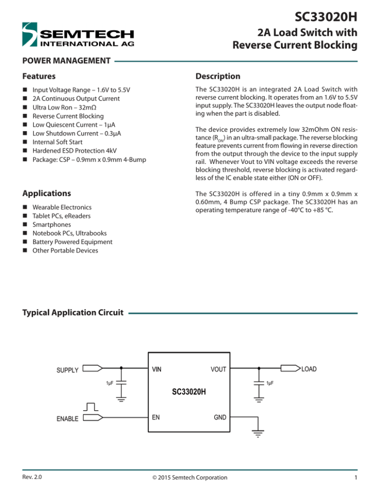
Typical Application Circuit
VIN
SUPPLY
1µF
ENABLE
Rev. 2.0
1µF
SC33020H
EN
LOAD
VOUT
GND
© 2015 Semtech Corporation
SC33020H
Pin Configuration
Ordering Information
TOP VIEW
VIEW
(BUMPS TOP
ON THE
BOTTOM)
(BUMPS ON THE BOTTOM)
A1
A2
B1
B2
Device
Package
SC33020HCSTRT
CSP 0.9mm x 0.9mm 4-bump
SC33020HCSEVB
Evaluation Board
Notes:
(1) Available in tape and reel only. A reel contains 5,000 devices.
(2) Lead-free package only. Device is WEEE and RoHS compliant, and
halogen free.
CSP 0.9x0.9, 4 Bump
Marking Information
Marking for the 0.9 x 0.9 mm CSP 4 Lead Package :
O = Pin 1 ID
nn = Part No. Code (Example: H4) - Reference Part No.
SC33020H
Absolute Maximum Ratings
Recommended Operating Conditions
VIN to GND (V). . . . . . . . . . . . . . . . . . . . . . . . . . . . . -0.3 to +6.0
Ambient Temperature Range (°C). . . . . . . . . . -40 < TA < +85
EN to GND (V). . . . . . . . . . . . . . . . . . . . . . . . . . . . . . -0.3 to +6.0
Maxiumum Output Current (A) . . . . . . . . . . . . . . . . . . . . . . . . 2
VOUT to GND (V). . . . . . . .. . . . . . . . . . . . . . . . -0.3 to (VVIN + 0.3)
VVIN (V). . . . . . . . . . . . . . . . . . . . . . . . . . . . . . . . . . . . . . . . . 1.6 to 5.5
ESD Protection Level HBM (kV). . . . . . . . . . . . . . . . . . . . . . . 4
(1)
Thermal Information
Thermal Resistance, Junction to Ambient(2)
CSP (°C/W). . . . . . . . . . . . . . . . . . . . . . . . . . . . . . . . . . . . . .
140
Maximum Junction Temperature (°C). . . . . . . . . . . . . . . +125
Storage Temperature Range (°C). . . . . . . . . . . . . -65 to +150
Peak IR Reflow Temperature (10s to 30s) (°C) . . . . . . . . +260
Exceeding the above specifications may result in permanent damage to the device or device malfunction. Operation outside of the parameters
specified in the Electrical Characteristics section is not recommended.
NOTES:
(1) Tested according to JEDEC standard JS-001-2012.
(2) Calculated from package in still air, mounted to 3 x 4.5 (in), 4 layer FR4 PCB with thermal vias under the exposed pad per JESD51 standards.
Electrical Characteristics
Unless noted otherwise, TA = 25°C for typical, -40°C < TA = TJ < +85°C for min and max, VIN = 2.8V, CIN = 1μF, COUT = 1μF, VEN = VVIN.
Parameter
Ron
Symbol
RON
Quiescent Current(1)
IQ
Shutdown Current
ISD
Conditions
Min
Typ
Max
Units
VIN =5.5V, IOUT = 200mA, VEN =1.5V
25
mΩ
VIN =4.3V, IOUT = 200mA, VEN =1.5V
28
mΩ
VIN =3.3V, IOUT = 200mA, VEN =1.5V
32
VIN =2.5V, IOUT = 200mA, VEN =1.5V
40
mΩ
VIN =1.6V, IOUT = 200mA, VEN =1.5V
65
mΩ
VIN=VEN,=3.6V, VOUT = open
1
3
µA
VEN=0, VOUT = open
0.3
2
μA
1.24
μA
VEN=0, VOUT = open, TA = 25°C
43
mΩ
Turn-on Delay Time(2)
TDT
VEN=1.5V, VIN=3.6V, IOUT=200mA, COUT=1μF
440
μs
Rising Time(2)
TRT
VEN=1.5V, VIN=3.6V, IOUT=200mA, COUT=1μF
640
μs
Reverse Blocking Current (IOUT)
RI
VEN=0V, VIN=0V, VOUT=5.5V
3
Reverse Blocking Threshold
RBT
VOUT=2.8V, VOUT − VIN
75
mV
Reverse Blocking Hysteresis
RBH
VOUT=2.8V, VOUT − VIN
25
mV
Reverse Blocking
13
µA
SC33020H
Electrical Characteristics (continued)
Parameter
Symbol
Conditions
Min
Typ
Max
Units
1.0
V
EN Digital Input
EN Input High Threshold
VEN-IH
EN Input Low Threshold
VEN-IL
EN Input Pull-Down Resistance
REN
0.4
V
7
MΩ
NOTES:
(1) IQ current includes EN pull-down current.
(2) For other TDT and TRT options, please contact SEMTECH.
SC33020H
Pin Descriptions
Pin#
Pin
Name
A1
VIN
Input supply voltage.
B1
EN
Enable input. A 7MΩ internal resistor is connected from this pin to GND. Drive HIGH to turn on the switch; drive
LOW to turn off the switch. When the EN pin is floated, the switch is OFF.
A2
OUT
Output voltage.
B2
GND
Ground.
Pin Function
Timing Diagram
Turn-on
Delay
Turn-off
Delay
VEN
VOUT
90%
10%
Rising
Time
Falling
Time
(Turn on time)=(Turn-on Delay)+(Rising Time)
SC33020H
TypicalTesting
Characteristics
condition: VIN=5.5V, Iout=2A (Pure
Testing condition: VIN=5.5V, Iout=2A,
C2=1uF, Pure Shut
Resistor,
Down25ɗ
by VIN
Start25ɗ
Up by VIN
Resistor), C2=1uF,
5.5Vin, 2A
5.5Vin, 2A
VIN
1V/div.
T1(Vin)
VOUT
1V/div.
Iout
VIN
1V/div.
VOUT
1V/div.
IOUT
1A/div.
IOUT
1A/div.
T1(Vin)
T2(Vout)
Iout
Time (2ms/div)
Time (2ms/div)
VIN
1V/div.
3.6Vin, 18 Ω
Start Up by EN
Testing condition: VIN=5.5V, 25 Ԩ,
Start UpPure
by ENResistor,
Iout=2A, C1=C2=1uF,
5.5Vin, 2.75 Ω
T1(Vin)
T2(Vout)
VIN
1V/div.
VOUT
1V/div.
IOUT
IIN
1A/div.
VOUT
1V/div.
EN
1.5V/div.
EN
3.6V/div.
IOUT
0.2A/div.
Time (0.2ms/div)
Time (0.2ms/div)
3.6Vin, 18 Ω
Shut Down by EN
VIN
1V/div.
VOUT
1V/div.
EN
Reverse Blocking
1.6Vin to 1.5Vin, 1.6Vout, 0A
VIN
0.3V/div.
VOUT
0.3V/div.
EN
3.6/div.
IIN
0.5A/div.
IOUT
0.2A/div.
Time (20µs/div)
Time (1ms/div)
SC33020H
Typical Characteristics, Cont.
On Resistance vs. Temperature
IOUT = 200mA
Ĺı
ijıı
1.6V
OnœŰůĩŮȟĪ
Resistance (mΩ)
ķı
Ķı
2.5V
ĵı
3.3V
4.3V
Ĵı
5.5V
ijı
1.6V
IJķı
IJĵı
IJijı
IJıı
2.5V
Ĺı
3.3V
4.3V
ķı
IJı
5.5V
ĵı
Įĵı
ijĶ
ĹĶ
Temperature (°C)
Įĵı
ijĶ
ŕŦŮűŦųŢŵŶųŦĩɗĪ
Shut Down Current vs. Temperature
Quiescent Current vs. Temperature
IJįĵ
ıįķ
IJįij
5.5V
Shutdown
Current (µA)
ŔũŶŵťŰŸůġńŶųųŦůŵĩŶłĪ
Quiescent
Current (µA)
ŒŶŪŦŴŤŦůŵġńŶųųŦůŵĩŶłĪ
ĹĶ
Temperature (°C)
ŕŦŮűŦųŢŵŶųŦĩɗĪ
IJįı
ıįĹ
3.3V
ıįķ
2.8V
ıįĵ
1.6V
ıįĶ
5.5V
3.3V
ıįĵ
2.8V
ıįĴ
ıįij
1.6V
ıįIJ
ıįij
ıįı
Įĵı
ijĶ
Temperature (°C)
ıįı
ĹĶ
Įĵı
ijĶ
Temperature (°C)
ŕŦŮűŦųŢŵŶųŦĩɗĪ
ĹĶ
ŕŦŮűŦųŢŵŶųŦĩɗĪ
EN Pull-Down Resistance vs. Temperature
EN HIGH Threshold vs. Temperature
2.8Vin
ĺıı
Ĺįı
EN Input
Pull-Down Resistance (MΩ)
ņŏġőŶŭŭťŰŸůġœŦŴŪŴŵŢůŤŦĩŎȟĪ
ņŏĩŮŗĪ (mV)
EN High Threshold
On Resistance vs. Temperature
IJĹı
ĸı
On œŰůĩŮȟĪ
Resistance (mΩ)
IOUT = 2A
ĹĶı
Ĺıı
5.5V
ĸĶı
3.6V
2.8V
ĸıı
ķĶı
1.6V
ķıı
ĸįĹ
ĸįķ
ĸįĵ
ĸįij
ĸįı
ķįĹ
ķįķ
ķįĵ
ķįij
ķįı
ĶĶı
Įĵı
ijĶ
Temperature
(°C)
ŕŦŮűŦųŢŵŶųŦĩɗĪ
ĹĶ
Įĵı
ijĶ
ĹĶ
Temperature
(°C)
ŕŦŮűŦųŢŵŶųŦĩɗĪ
SC33020H
Typical Characteristics, Cont.
Rising Time vs. Temperature
Turn-on Delay Time vs. Temperature
ijĶıı
IJķıı
Turn-On Rising Time (µs)
IJijıı
1.6V
ŕŶųůĮŐŧŧġŅŦŭŢźġŕŪŮŦĩŶŔĪ
ŕŶųůĮŐůġŅŦŭŢźġŕŪŮŦĩŶŔĪ
Turn-On Delay Time (µs)
IJĵıı
ijııı
IJĶıı
IJııı
3.6V
Ķıı
5.5V
ijĶ
Temperature (°C)
Ĺıı
3.6V
ķıı
5.5V
ĵıı
ijıı
ı
Įĵı
1.6V
IJııı
ı
ĹĶ
Įĵı
ijĶ
Temperature (°C)
ŕŦŮűŦųŢŵŶųŦĩɗĪ
ŕŦŮűŦųŢŵŶųŦĩɗĪ
Reverse Blocking Current vs. Temperature
Turn-off Time vs. Temperature
ĴĶ
1.6V
ijĶ
ijı
œŦŷŦųŴŦġŃŭŰŤŬŪůŨġńŶųųŦůŵĩŶłĪ
Turn-Off Time (µs)
ŕŶųůĮŐŧŧġŅŦŭŢźġŕŪŮŦĩŶŔĪ
Reverse Blocking Current (µA)
ķ
Ĵı
3.6V
IJĶ
3.6V
IJı
ĹĶ
5.5V
Ķ
EN = Low
Ķ
ĵ
Ĵ
ij
IJ
ı
ı
Įĵı
ijĶ
Temperature (°C)
ĹĶ
ŕŦŮűŦųŢŵŶųŦĩɗĪ
Įĵı
ijĶ
ĹĶ
Temperature (°C)
ŕŦŮűŦųŢŵŶųŦĩɗĪ
Reverse Blocking Threshold and Hysteresis
vs. Temperture
ĺı
Ůŗ (mV)
Reverse Blocking
Ĺı
Threshold
ĸı
ķı
Ķı
ĵı
Hysteresis
Ĵı
ijı
Įĵı
ijĶ
ĹĶ
Temperature
(°C)
ŕŦŮűŦųŢŵŶųŦĩɗĪ
SC33020H
Block Diagram
REVERSE BLOCKING
VOUT
VIN (1.6V to 5.5V)
C1
Slew Rate
Control
EN
C2
ILoad
(Up to 2A)
SC33020H
GND
SC33020H
Application Information
Operation
The SC33020H is an integrated high-side PMOS load
switch that is designed to support up to 2A continuous
output current and operates from an input voltage from
1.6V to 5.5V. The internal PMOS pass element has a very
low ON resistance of 32mΩ (typical) at VIN = 3.3V. The
SC33020H also provides ultra-low shutdown and quiescent current for extended battery life during shutdown
and standby conditions.
An internal soft start circuit is used to control the start-up
time of the load switch to reduce inrush current during
start up.
Enable
The EN pin controls the ON/OFF state of the load switch.
Pulling the EN pin HIGH turns on the load switch. Pulling
the EN pin LOW turns off the load switch. The EN pin
incorporates a 7MΩ (typical) pull-down resistor, so that
when the EN pin is floating the SC33020H is disabled.
Reverse Blocking
The SC33020H integrates a reverse current blocking circuit
to prevent current flow from VOUT to VIN during both ON
and OFF states. The reverse current blocking circuit is
active when voltage is present on either the VIN or the
VOUT. A comparator is used to sense and compare the
VOUT voltage to the VIN voltage. Whenever the VOUT
voltage is 75mV (typical at 25°C) higher than VIN, the
Reverse Blocking circuit is triggered and reverse current is
blocked from VOUT to VIN. Please note that when 0 <
VOUT - VIN < 75mV (typical at 25°C), some small reverse
current is possible. An example is shown in Fig. 1. Usually,
worst case for reverse current occurs at elevated input
voltages and reduced temperatures.
The following formula can be used to calculate the reverse
peak current before the Reverse Blocking circuit is triggered.
IRC = VRBT
RON
IRC - Reverse peak current. R ON - On-Resistance, (Usually, is smaller resistance at
higher VIN and lower temperature.)
VRBT - Reverse voltage threshold.
IRC is the amount of reverse current,
RON is the on-resistance, on There is smaller resistance at larger VIN and lower ambient temperature
VBT is the reverse voltage threshold.
VOUT
VRBT
IRC
VIN
REVERSE CURRENT
Figure 1
Input Capacitor
In order to reduce the effect of voltage drop, noise and
bounce at the VIN pin, a filter/decoupling capacitor
between VIN to GND is recommended. A 1µF ceramic
capacitor is sufficient for most application conditions.
However, it should be noted that suppressing bounce at
input loop after EN is changed from HIGH to LOW can
require greater capacitor values depending on particular
designs.
In circuit design, ceramic capacitors should be derated for
operating temperature and voltage. For applications up to
3.6V, capacitors should be rated at 6.3V or higher. For applications up to 5.5V, capacitors should be rated at 10V or
higher.
Output Capacitor
A 1µF ceramic capacitor is normally used at the VOUT pin
to filter noise. If a larger output capacitance value is used,
the input inrush current should be considered because
the power-on transient is also dependent on the output
capacitor value. Please use the same derating criteria for
the output capacitor selection.
Board Layout Considerations
Fig. 2 shows a typical application circuit with PCB inductance on the circuit board. An important objective of the
layout is to minimize the PCB inductance by reducing the
length and increasing the width of the traces. PCB inductance can affect circuit performance during turn-off, load
transients, and Reverse Blocking. Fig. 2 shows three current
loops during the opening or closing of the load switch.
The magnitude of the voltage ringing at VIN or VOUT pin
10
SC33020H
Application Information, Cont.
is related to the PCB stray inductance and the placement
of the capacitors. The input capacitor C1 and output
capacitor C2 need to be placed close to the SC33020H. It
is important to keep the voltage ringing below the
maximum voltage rating of the SC33020H.
LPCB
LPCB
+
-
IIN
VIN
VOUT
C1
1uF
LPCB
LPCB
C2
1uF
SC33020H
IOUT
RL
GND
ISW
LPCB
Figure 2 - PCB Circuit with Equivalent Parasitic
Inductance
Evaluation Board Information
The Top Layer and Bottom Layer of a standard evaluation
board are shown in Fig. 3 and Fig. 4, respectively.
Both T1 and T2 test points are Kelvin connections which
can be used to minimize the measurement error of RON.
To enable the part, a jumper can be used between VIN
and EN on J1. To disable the part, a jumper can be connected between EN and GND on J1. C3 is an optional
solution to improve ringing at input rail during turn-off
and reverse blocking conditions.
11
SC33020H
Top Layer, SC33020H
DBN461!W!21/6!;!Uiv!Bvh!39!27;3:;2:!3125!.!)Voujumfe*
Figure 3
Bottom Layer, SC33020H
DBN461!W!21/6!;!Uiv!Bvh!39!27;41;22!3125!.!)Voujumfe*
Figure 4
12
SC33020H
Outline Drawing — CSP 0.9mm X 0.9mm, 4 Lead
13
SC33020H
Land Pattern — CSP 0.9mm X 0.9mm, 4 Lead
14
SC33020H
© Semtech 2015
All rights reserved. Reproduction in whole or in part is prohibited without the prior written consent of the copyright
owner. The information presented in this document does not form part of any quotation or contract, is believed to be
accurate and reliable and may be changed without notice. No liability will be accepted by the publisher for any consequence of its use. Publication thereof does not convey nor imply any license under patent or other industrial or intellectual property rights. Semtech assumes no responsibility or liability whatsoever for any failure or unexpected operation
resulting from misuse, neglect improper installation, repair or improper handling or unusual physical or electrical stress
including, but not limited to, exposure to parameters beyond the specified maximum ratings or operation outside the
specified range.
SEMTECH PRODUCTS ARE NOT DESIGNED, INTENDED, AUTHORIZED OR WARRANTED TO BE SUITABLE FOR USE IN LIFESUPPORT APPLICATIONS, DEVICES OR SYSTEMS OR OTHER CRITICAL APPLICATIONS. INCLUSION OF SEMTECH PRODUCTS
IN SUCH APPLICATIONS IS UNDERSTOOD TO BE UNDERTAKEN SOLELY AT THE CUSTOMER’S OWN RISK. Should a customer
purchase or use Semtech products for any such unauthorized application, the customer shall indemnify and hold
Semtech and its officers, employees, subsidiaries, affiliates, and distributors harmless against all claims, costs damages
and attorney fees which could arise.
Notice: All referenced brands, product names, service names and trademarks are the property of their respective
owners.
Contact Information
Taiwan
Tel: 886-2-2748-3380
Fax: 886-2-2748-3390
Switzerland
Tel: 41-32-729-4000
Fax: 41-32-729-4001
Korea
Tel: 82-2-527-4377
Fax: 82-2-527-4376
United Kingdom
Tel: 44-1794-527-600
Fax: 44-1794-527-601
Shanghai
Tel: 86-21-6391-0830
Fax: 86-21-6391-0831
France
Tel: 33-(0)169-28-22-00
Fax: 33-(0)169-28-12-98
Japan
Tel: 81-3-6408-0950
Fax: 81-3-6408-0951
Germany
Tel: 49-(0)8161-140-123
Fax: 49-(0)8161-140-124
www.semtech.com
15
