HT82V36 - 16-Bit CCD/CIS Analog Signal Processor
advertisement
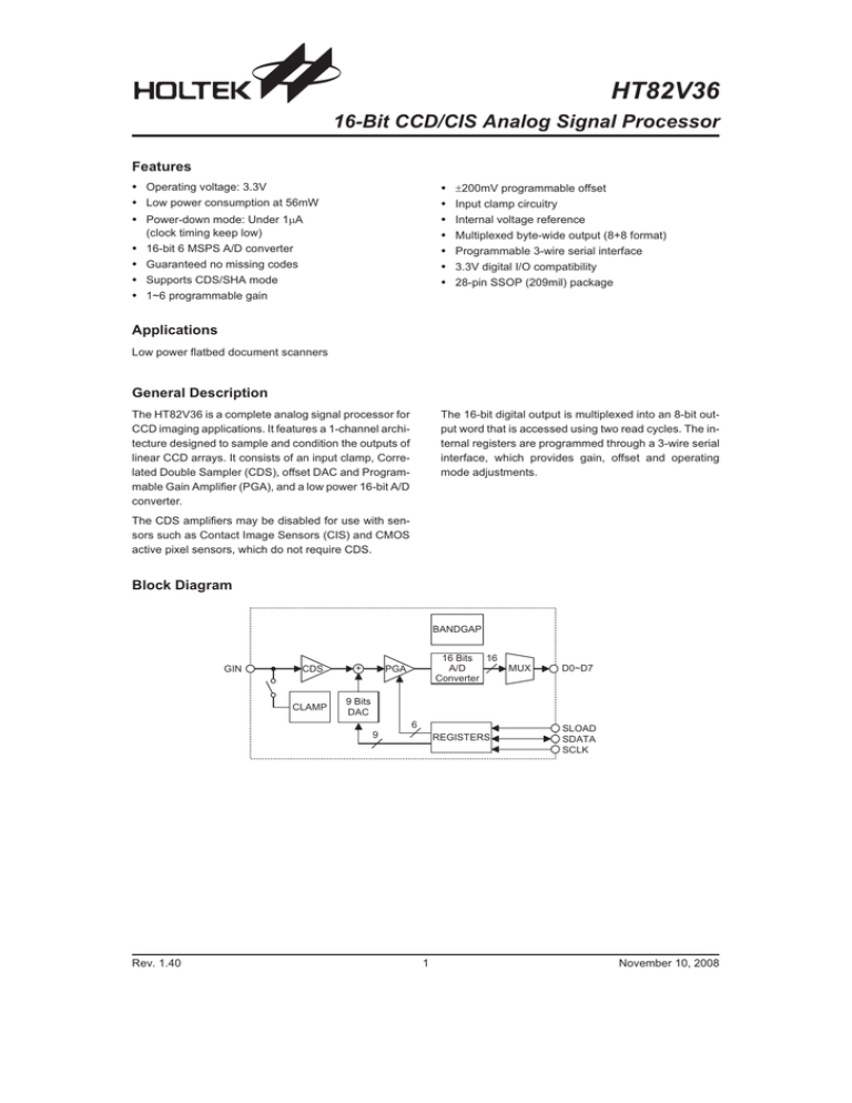
HT82V36 16-Bit CCD/CIS Analog Signal Processor Features · Operating voltage: 3.3V · ±200mV programmable offset · Low power consumption at 56mW · Input clamp circuitry · Power-down mode: Under 1mA · Internal voltage reference (clock timing keep low) · Multiplexed byte-wide output (8+8 format) · 16-bit 6 MSPS A/D converter · Programmable 3-wire serial interface · Guaranteed no missing codes · 3.3V digital I/O compatibility · Supports CDS/SHA mode · 28-pin SSOP (209mil) package · 1~6 programmable gain Applications Low power flatbed document scanners General Description The 16-bit digital output is multiplexed into an 8-bit output word that is accessed using two read cycles. The internal registers are programmed through a 3-wire serial interface, which provides gain, offset and operating mode adjustments. The HT82V36 is a complete analog signal processor for CCD imaging applications. It features a 1-channel architecture designed to sample and condition the outputs of linear CCD arrays. It consists of an input clamp, Correlated Double Sampler (CDS), offset DAC and Programmable Gain Amplifier (PGA), and a low power 16-bit A/D converter. The CDS amplifiers may be disabled for use with sensors such as Contact Image Sensors (CIS) and CMOS active pixel sensors, which do not require CDS. Block Diagram B A N D G A P G IN C D S C L A M P + 1 6 M U X D 0 ~ D 7 9 B its D A C 9 Rev. 1.40 1 6 B its A /D C o n v e rte r P G A 6 R E G IS T E R S 1 S L O A D S D A T A S C L K November 10, 2008 HT82V36 Pin Assignment C D S C L K 1 1 2 8 A V D D C D S C L K 2 2 2 7 A V S S A D C C L K 3 2 6 N C O E 4 2 5 O F F S E T D R V D D 5 2 4 V IN G D R V S S 6 2 3 C M L D 7 (M S B ) 7 2 2 N C D 6 8 2 1 R E F T D 5 9 2 0 R E F B D 4 1 0 1 9 A V S S D 3 1 1 1 8 A V D D D 2 1 2 1 7 S L O A D D 1 1 3 1 6 S C L K D 0 (L S B ) 1 4 1 5 S D A T A H T 8 2 V 3 6 2 8 S S O P -A Pin Description Pin No. Pin Name I/O Description 1 CDSCLK1 DI CDS reference clock pulse input 2 CDSCLK2 DI CDS data clock pulse input 3 ADCCLK DI A/D sample clock input 4 OE DI Output enable, active low 5 DRVDD P Digital driver power 6 DRVSS P Digital driver ground 7~14 D7~D0 DO 15 SDATA DI/DO 16 SCLK DI 17 SLOAD DI Serial interface load pulse 18, 27 AVSS P Analog ground 19, 28 AVDD P 20 REFB AO 21 REFT AO Reference decoupling 23 CML AO Internal reference output 24 VING AI Analog input 25 OFFSET AO Clamp bias level decoupling 22, 26 NC ¾ No connection Digital data output Serial data input/output Clock input for serial interface Analog supply Reference decoupling Absolute Maximum Ratings Supply Voltage ..........................VSS-0.3V to VSS+3.6V Storage Temperature ...........................-50°C to 125°C Input Voltage .............................VSS-0.3V to VDD+0.3V Operating Temperature ..........................-25°C to 75°C Note: These are stress ratings only. Stresses exceeding the range specified under ²Absolute Maximum Ratings² may cause substantial damage to the device. Functional operation of this device at other conditions beyond those listed in the specification is not implied and prolonged exposure to extreme conditions may affect device reliability. Rev. 1.40 2 November 10, 2008 HT82V36 D.C. Characteristics Symbol Parameter Test Conditions VDD Conditions Min. Typ. Max. Unit Logic Inputs VIH High Level Input Voltage ¾ ¾ 0.8´VDD ¾ ¾ V VIL Low Level Input Voltage ¾ ¾ ¾ ¾ 0.2´VDD V IIH High Level Input Current ¾ ¾ ¾ 10 ¾ mA IIL Low Level Input Current ¾ ¾ ¾ 10 ¾ mA CIN Input Capacitance ¾ ¾ ¾ 10 ¾ pF V Logic Outputs VOH High Level Output Voltage ¾ ¾ VDD-0.5 ¾ ¾ VOL Low Level Output Voltage ¾ ¾ ¾ ¾ 0.5 V IOH High Level Output Current ¾ ¾ ¾ 1 ¾ mA IOL Low Level Output Current ¾ ¾ ¾ 1 ¾ mA Min. Typ. Max. Unit ¾ ¾ MHz A.C. Characteristics Symbol Parameter Test Conditions VDD Conditions ¾ ¾ 6 ADC Resolution ¾ ¾ ¾ 16 ¾ Integral Nonlinear (INL) ¾ ¾ ¾ ±16 ¾ LSB Differential Nonlinear (DNL) ¾ ¾ -1 ¾ 2 LSB Offset Error ¾ ¾ -100 TBD 100 mV Gain Error ¾ ¾ ¾ TBD ¾ %FSR Maximum Conversion Rate tMAX CDS/SHA Mode Accuracy (Entire Signal Path) Analog Inputs RFS Full-scale Input Range ¾ ¾ 1.3 1.4 1.6 Vp-p Vi Input Limits ¾ ¾ AVDD-0.3 ¾ AVDD+0.3 V Ci Input Capacitance ¾ ¾ ¾ TBD ¾ pF Ii Input Current ¾ ¾ ¾ TBD ¾ mA PGA Gain at Minimum ¾ ¾ ¾ 1 ¾ V/V PGA Gain at Maximum ¾ ¾ ¾ 5.85 ¾ V/V PGA Gain Resolution ¾ ¾ ¾ 6 ¾ Bits Amplifiers Programmable Offset at Minimum ¾ ¾ ¾ -200 ¾ mV Programmable Offset at Maximum ¾ ¾ ¾ 200 ¾ mV Offset Resolution ¾ ¾ ¾ 9 ¾ Bits ¾ ¾ 0 ¾ 70 °C Temperature Range tA Operating Power Supplies VADD AVDD ¾ ¾ 3 3.3 3.6 V VDRDD DRVDD ¾ ¾ 3 3.3 3.6 V ¾ ¾ ¾ 56 ¾ mW Power Consumption Ptot Rev. 1.40 Total Power Consumption 3 November 10, 2008 HT82V36 Timing Specification Symbol Parameter Min. Typ. Max. Unit ¾ ns Clock Parameters tADCLK Pixel Rate Clock 166 ¾ tADH ADCCLK Pulse High Width 80 ¾ ns tADL ADCCLK Pulse Low Width 80 ¾ ns tC1 CDSCLK1 Pulse Width 20 ¾ ¾ ns tC2 CDS Mode CDSCLK2 Pulse Width 20 ¾ ¾ ns tC3 SHA Mode CDSCLK2 Pulse Width 40 ¾ ¾ ns tC2ADF CDSCLK2 Falling to ADCCLK Falling 60 ¾ ¾ ns tADFC1 ADCCLK Falling to CDSCLK1 Rising 2 ¾ ¾ ns tADFC2 ADCCLK Falling to CDSCLK2 Rising 2 ¾ ¾ ns tAD Analog Sampling Delay 5 ¾ ¾ ns Serial Interface fSCLK Maximum SCLK Frequency 10 ¾ ¾ MHz tLS SLOAD to SCLK Setup Time 10 ¾ ¾ ns tLH SCLK to SLOAD Hold Time 10 ¾ ¾ ns tDS SDATA to SCLK Rising Setup Time 10 ¾ ¾ ns tDH SCLK Rising to SDATA Hold Time 10 ¾ ¾ ns tRDV Falling to SDATA Valid 10 ¾ ¾ ns Output Delay ¾ 8 ¾ ns Latency (Pipeline Delay) ¾ 9 ¾ Cycles Data Output tOD Functional Description The offset error is the deviation of the actual first code transition level from the ideal level. Integral Nonlinear (INL) Integral nonlinear error refers to the deviation of each individual code from a line drawn from zero scale through positive full scale. The point used as zero scale occurs 1 /2 LSB before the first code transition. Positive full scale is defined as a level 1/2 LSB beyond the last code transition. The deviation is measured from the middle of each particular code to the true straight line. Gain Error The last code transition should occur for an analog value 1/2 LSB below the nominal full-scale voltage. Gain error is the deviation of the actual difference between first and last code transitions and the ideal difference between the first and last code transitions. Differential Nonlinear (DNL) Aperture Delay An ideal ADC exhibits code transitions that are exactly 1 LSB apart. DNL is the deviation from this ideal value. Thus every code must have a finite width. No missing codes guaranteed to 16-bit resolution indicates that all 4096 codes, respectively, must be present over all operating ranges. The aperture delay is the time delay that occurs when a sampling edge is applied to the HT82V36 until the actual sample of the input signal is held. Both CDSCLK1 and CDSCLK2 sample the input signal during the transition from high to low, so the aperture delay is measured from each clock¢s falling edge to the instant the actual internal sample is taken. Offset Error The first ADC code transition should occur at a level 1/2 LSB above the nominal zero scale voltage. Rev. 1.40 4 November 10, 2008 HT82V36 Internal Register Descriptions Address Data Bits Register Name A2 A1 A0 D8 D7 D6 D5 D4 Configuration 0 0 0 0 0 1 1 CDS on Reserved 0 0 1 Reserved 0 1 0 PGA 0 1 1 X 0 0 MSB Reserved 1 0 0 Reserved 1 0 1 Offset 1 1 0 Reserved 1 1 1 D3 D2 D1 D0 Enable Output 1byte Clamp Power Delay out Voltage Down LSB MSB LSB Internal Register Map D8 D7 D6 D5 D4 Set to 0 Set to 0 Set to 1 Set to 1 D3 D2 D1 D0 CDS operation Clamp bias Power-down 1 byte out Output delay (High-byte only) 1=CDS mode* 1=2.5V* 1=On 1=On 0=SHA mode 0=Off (Normal)* 0=Off* 0=2V 1=On 0=Off* Configuration Register Settings Note: * Power-on default value PGA Gain Register Bits D7 and D6 in the register must be set low, and bits D5 through D0 control the gain range in 64 increments. See figure for a graph of the PGA gain versus PGA register code. The coding for the PGA register is straight binary, with an all zero words corresponding to the minimum gain setting (1x) and an all one word corresponding to the maximum gain setting (5.85x). The PGA has a gain range from 1x (0dB) to 5.85x (15.3dB), adjustable in 64 steps. The Figure shows the PGA gain as a function of the PGA register code. Although the gain curve is approximately linear in dB, the gain in V/V varies in non5.85 linear proportion with the register code, according to the following the equation: Gain= 63 - G 1+ 4.85 ´ ´ ( ) 63 Where G is the decimal value of the gain register contents, and varies from 0 to 63. 5 .8 5 1 2 5 .0 4 .0 6 3 .0 3 2 .0 G A IN -d B ( 9 0 G A IN -V /V ( ) ) 1 5 1 .0 0 4 8 1 2 1 6 2 0 2 4 2 8 3 2 3 6 4 0 4 4 4 8 5 2 5 6 6 0 6 3 P G A r e g is te r v a lu e - - D e c im a l PGA Gain Transfer Function Rev. 1.40 5 November 10, 2008 HT82V36 D8 D7 D6 D5 D4 Set to 0 Set to 0 Set to 0 MSB 0 0 0 0 0 0 0 0 0 0 0 0 0 0 0 0 1 1 1 1 D3 D2 D1 D0 Gain (V/V) Gain (dB) 1.0 1.013 . . . 5.43 5.85 0.0 0.12 . . . 14.7 15.3 LSB 0 0 . . . 1 1 0 0 0 0 0* 1 1 1 1 1 0 1 PGA Gain Register Settings Note: * Power-on default value Offset Register Bits D8 through D0 control the offset range from -200mV to 200mV in 512 increments. The coding for the offset registers is sign magnitude, with D8 as the sign bit. The Table shows the offset range as a function of the bits D8 through D0. D8 D7 D6 D5 D4 D3 D2 D1 D0 MSB Offset (mV) LSB 0 0 0 0 0 0 0 0 0 0 0 1 1 1 0 0 1 0 0 1 0 0 1 0 0 1 1 1 1 1 0 0 . . . 1 0 0 . . . 1 0 0 0 0 0* 1 1 0 0 1 0 0 1 0 1 1 1 1 0 0.78 . . . 200 0 -0.78 . . . -200 Note: * Power-on default value Timing Diagrams S D A T A A 2 R /W b tD A 1 A 0 H tD D 8 D 7 D 6 D 5 D 4 D 3 D 2 D 1 D 0 S S C L K tL tL S H S L O A D Serial Write Operation Timing S D A T A R /W b A 2 A 1 A 0 D 8 tR D 7 D 6 D 5 D 4 D 3 D 2 D 1 D 0 D V S C L K tL tL S H S L O A D Serial Read Operation Timing Rev. 1.40 6 November 10, 2008 HT82V36 P ix e l (N + 3 ) P ix e l (N + 4 ) P ix e l (N + 5 ) P ix e l (N + 6 ) P ix e l (N + 7 ) P ix e l (N + 8 ) P ix e l (N + 9 ) P ix e l (N + 1 0 ) A n a lo g In p u t tA tC D 1 C D S C L K 1 tC 2 C D S C L K 2 tA tC F C 1 tA 2 A D F tA D C L K tA D L D H A D C C L K tO O u tp u t D a ta D 7 ~ D 0 D P ix e l P ix e l P ix e l P ix e l P ix e l P ix e l P ix e l P ix e l P ix e l P ix e l P ix e l P ix e l P ix e l P ix e l P ix e l P ix e l P ix e l (N -7 ) (N -6 ) (N -6 ) (N -5 ) (N -5 ) (N -4 ) (N -4 ) (N -3 ) (N -3 ) (N -2 ) (N -2 ) (N -1 ) (N -1 ) (N ) (N ) (N + 1 ) (N + 1 ) L o w B y te H ig h B y te L o w B y te H ig h B y te L o w B y te H ig h B y te H ig h B y te L o w B y te H ig h B y te L o w B y te L o w B y te H ig h B y te L o w B y te H ig h B y te L o w B y te H ig h B y te L o w B y te 1-Channel CDS Mode Timing P ix e l (N + 5 ) P ix e l (N + 4 ) P ix e l (N + 6 ) P ix e l (N + 7 ) A n a lo g In p u t tA D tC 3 tC 2 A D F P ix e l (N + 9 ) P ix e l (N + 8 ) P ix e l (N + 1 1 ) P ix e l (N + 1 0 ) C D S C L K 2 tA D C L K tA tA D F C 2 D H tA D L A D C C L K tO O u tp u t D a ta D 7 ~ D 0 D P ix e l P ix e l P ix e l P ix e l P ix e l P ix e l P ix e l P ix e l P ix e l P ix e l P ix e l P ix e l P ix e l P ix e l P ix e l P ix e l P ix e l (N -7 ) (N -6 ) (N -6 ) (N -5 ) (N -5 ) (N -4 ) (N -4 ) (N -3 ) (N -3 ) (N -2 ) (N -2 ) (N -1 ) (N -1 ) (N ) (N ) (N + 1 ) (N + 1 ) L o w B y te H ig h B y te L o w B y te H ig h B y te L o w B y te H ig h B y te H ig h B y te L o w B y te H ig h B y te L o w B y te L o w B y te H ig h B y te L o w B y te H ig h B y te L o w B y te H ig h B y te L o w B y te 1-Channel SHA Mode Timing Rev. 1.40 7 November 10, 2008 HT82V36 Application Circuits The recommended circuit configuration for 1-channel CDS mode operation is shown below. The recommended input coupling capacitor value is 0.1mF (see circuit operation section for more details). A single ground plane is recommended for the HT82V36. A separate power supply may be used for DRVDD, the digital driver supply, but this supply pin should still be decoupled to the same ground plane as the rest of the HT82V36. The loading of the digital outputs should be minimized, either by using short traces to the digital ASIC, or by using external digital buffers. All 0.1mF decoupling capacitors should be located as close as possible to the HT82V36 pins. V 1 2 3 C D S C L K 1 A V D D C D S C L K 2 A V S S 3 .3 V A D C C L K 4 O E 5 6 7 9 1 0 1 1 1 2 1 3 1 4 O F F S E T D R V D D V IN G D R V S S C M L D 7 (M S B ) 8 N C N C D 6 R E F T D 5 R E F B D 4 A V S S D 3 A V D D D 2 S L O A D D 1 S C L K D 0 (L S B ) S D A T A D D 0 .1 m F 2 8 2 7 2 6 0 .1 m F 2 5 2 4 0 .1 m F 2 3 0 .1 m F In p u t 1 .0 m F 2 2 2 1 0 .1 m F 2 0 0 .1 m F 1 0 m F 1 9 1 8 0 .1 m F 0 .1 m F 1 7 3 .3 V 1 6 1 5 H T 8 2 V 3 6 (C D S M o d e ) V 1 2 3 C D S C L K 1 A V D D C D S C L K 2 A V S S 3 .3 V A D C C L K 4 5 O E 6 7 D R V D D V IN G D R V S S C M L D 7 (M S B ) 8 9 1 0 1 1 1 2 1 3 1 4 N C O F F S E T N C D 6 R E F T D 5 R E F B D 4 A V S S D 3 A V D D D 2 S L O A D D 1 S C L K D 0 (L S B ) S D A T A 2 8 D D 0 .1 m F 2 7 2 6 2 5 2 4 2 3 D C L e v e l In p u t 0 .1 m F 2 2 2 1 0 .1 m F 2 0 1 9 1 8 1 7 1 6 0 .1 m F 1 0 m F 0 .1 m F 0 .1 m F 3 .3 V 1 5 H T 8 2 V 3 6 (S H A M o d e ) Note: For the SHA Mode, all of the above considerations also apply, except that the analog input signal is directly connected to the HT82V36 without using a coupling capacitor. The OFFSET pin should be grounded if the input to the HT82V36 is to be referenced to ground, or a dc offset voltage should be applied to the OFFSET pin in situation where a coarse offset needs to be removed from the input. Rev. 1.40 8 November 10, 2008 HT82V36 Package Information 28-pin SSOP (209mil) Outline Dimensions 1 5 2 8 A B 1 4 1 C C ' G H D E Symbol Rev. 1.40 a F Dimensions in mil Min. Nom. Max. A 291 ¾ 323 B 196 ¾ 220 C 9 ¾ 15 C¢ 396 ¾ 407 D 65 ¾ 73 E ¾ 25.59 ¾ F 4 ¾ 10 G 26 ¾ 34 H 4 ¾ 8 a 0° ¾ 8° 9 November 10, 2008 HT82V36 Product Tape and Reel Specifications Reel Dimensions D T 2 A C B T 1 SSOP 28S (209mil) Symbol Description A Reel Outer Diameter Dimensions in mm 330.0±1.0 B Reel Inner Diameter 100.0±1.5 C Spindle Hole Diameter 13.0+0.5/-0.2 D Key Slit Width T1 Space Between Flange 28.4+0.3/-0.2 T2 Reel Thickness 31.1 (max.) Rev. 1.40 2.0±0.5 10 November 10, 2008 HT82V36 Carrier Tape Dimensions P 0 D P 1 t E F W C D 1 B 0 P K 0 A 0 R e e l H o le IC p a c k a g e p in 1 a n d th e r e e l h o le s a r e lo c a te d o n th e s a m e s id e . SSOP 28S (209mil) Symbol Description Dimensions in mm W Carrier Tape Width 24.0±0.3 P Cavity Pitch 12.0±0.1 E Perforation Position 1.75±0.1 F Cavity to Perforation (Width Direction) 11.5±0.1 D Perforation Diameter 1.5+0.1/-0.0 D1 Cavity Hole Diameter 1.50+0.25/-0.00 P0 Perforation Pitch 4.0±0.2 P1 Cavity to Perforation (Length Direction) 2.0±0.1 A0 Cavity Length 8.4±0.1 B0 Cavity Width 10.65±0.10 K0 Cavity Depth 2.4±0.1 t Carrier Tape Thickness 0.30±0.05 C Cover Tape Width 21.3±0.1 Rev. 1.40 11 November 10, 2008 HT82V36 Holtek Semiconductor Inc. (Headquarters) No.3, Creation Rd. II, Science Park, Hsinchu, Taiwan Tel: 886-3-563-1999 Fax: 886-3-563-1189 http://www.holtek.com.tw Holtek Semiconductor Inc. (Taipei Sales Office) 4F-2, No. 3-2, YuanQu St., Nankang Software Park, Taipei 115, Taiwan Tel: 886-2-2655-7070 Fax: 886-2-2655-7373 Fax: 886-2-2655-7383 (International sales hotline) Holtek Semiconductor (China) Inc. (Dongguan Sales Office) Building No. 10, Xinzhu Court, (No. 1 Headquarters), 4 Cuizhu Road, Songshan Lake, Dongguan, China 523808 Tel: 86-769-2626-1300 Fax: 86-769-2626-1311 Holtek Semiconductor (USA), Inc. (North America Sales Office) 46729 Fremont Blvd., Fremont, CA 94538, USA Tel: 1-510-252-9880 Fax: 1-510-252-9885 http://www.holtek.com Copyright Ó 2008 by HOLTEK SEMICONDUCTOR INC. The information appearing in this Data Sheet is believed to be accurate at the time of publication. However, Holtek assumes no responsibility arising from the use of the specifications described. The applications mentioned herein are used solely for the purpose of illustration and Holtek makes no warranty or representation that such applications will be suitable without further modification, nor recommends the use of its products for application that may present a risk to human life due to malfunction or otherwise. Holtek¢s products are not authorized for use as critical components in life support devices or systems. Holtek reserves the right to alter its products without prior notification. For the most up-to-date information, please visit our web site at http://www.holtek.com.tw. Rev. 1.40 12 November 10, 2008
