Freescale Semiconductor
Application Note
AN1318
Rev 2, 05/2005
Interfacing Semiconductor Pressure
Sensors to Microcomputers
by: Warren Schultz
Discrete Applications Engineering
INTRODUCTION
The most popular silicon pressure sensors are
piezoresistive bridges that produce a differential output
voltage in response to pressure applied to a thin silicon
diaphragm. Output voltage for these sensors is generally 25 to
50 mV full scale. Interface to microcomputers, therefore,
generally involves gaining up the relatively small output
voltage, performing a differential to single ended conversion,
and scaling the analog signal into a range appropriate for
analog to digital conversion. Alternately, the analog pressure
signal can be converted to a frequency modulated 5 V
waveform or 4-20 mA current loop, either of which is relatively
immune to noise on long interconnect lines.
A variety of circuit techniques that address interface design
are presented. Sensing amplifiers, analog to digital
conversion, frequency modulation and 4-20 mA current loops
are considered.
PRESSURE SENSOR BASICS
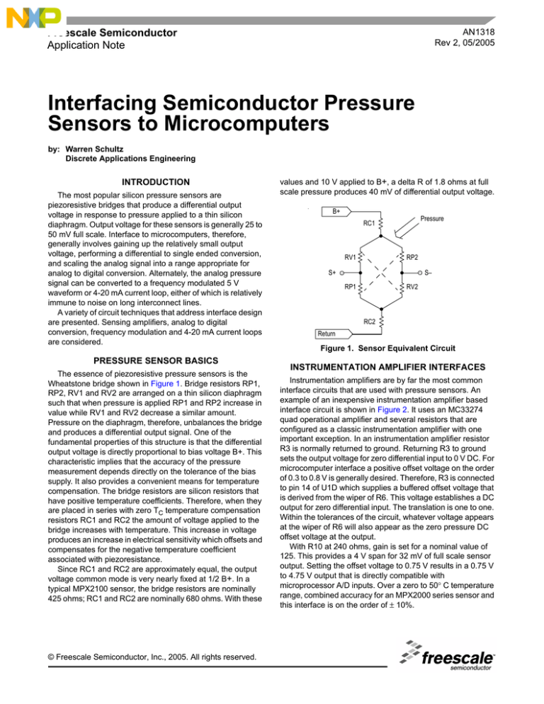
The essence of piezoresistive pressure sensors is the
Wheatstone bridge shown in Figure 1. Bridge resistors RP1,
RP2, RV1 and RV2 are arranged on a thin silicon diaphragm
such that when pressure is applied RP1 and RP2 increase in
value while RV1 and RV2 decrease a similar amount.
Pressure on the diaphragm, therefore, unbalances the bridge
and produces a differential output signal. One of the
fundamental properties of this structure is that the differential
output voltage is directly proportional to bias voltage B+. This
characteristic implies that the accuracy of the pressure
measurement depends directly on the tolerance of the bias
supply. It also provides a convenient means for temperature
compensation. The bridge resistors are silicon resistors that
have positive temperature coefficients. Therefore, when they
are placed in series with zero TC temperature compensation
resistors RC1 and RC2 the amount of voltage applied to the
bridge increases with temperature. This increase in voltage
produces an increase in electrical sensitivity which offsets and
compensates for the negative temperature coefficient
associated with piezoresistance.
Since RC1 and RC2 are approximately equal, the output
voltage common mode is very nearly fixed at 1/2 B+. In a
typical MPX2100 sensor, the bridge resistors are nominally
425 ohms; RC1 and RC2 are nominally 680 ohms. With these
© Freescale Semiconductor, Inc., 2005. All rights reserved.
values and 10 V applied to B+, a delta R of 1.8 ohms at full
scale pressure produces 40 mV of differential output voltage.
B+
Pressure
RC1
RV1
RP2
S+
S–
RP1
RV2
RC2
Return
Figure 1. Sensor Equivalent Circuit
INSTRUMENTATION AMPLIFIER INTERFACES
Instrumentation amplifiers are by far the most common
interface circuits that are used with pressure sensors. An
example of an inexpensive instrumentation amplifier based
interface circuit is shown in Figure 2. It uses an MC33274
quad operational amplifier and several resistors that are
configured as a classic instrumentation amplifier with one
important exception. In an instrumentation amplifier resistor
R3 is normally returned to ground. Returning R3 to ground
sets the output voltage for zero differential input to 0 V DC. For
microcomputer interface a positive offset voltage on the order
of 0.3 to 0.8 V is generally desired. Therefore, R3 is connected
to pin 14 of U1D which supplies a buffered offset voltage that
is derived from the wiper of R6. This voltage establishes a DC
output for zero differential input. The translation is one to one.
Within the tolerances of the circuit, whatever voltage appears
at the wiper of R6 will also appear as the zero pressure DC
offset voltage at the output.
With R10 at 240 ohms, gain is set for a nominal value of
125. This provides a 4 V span for 32 mV of full scale sensor
output. Setting the offset voltage to 0.75 V results in a 0.75 V
to 4.75 V output that is directly compatible with
microprocessor A/D inputs. Over a zero to 50° C temperature
range, combined accuracy for an MPX2000 series sensor and
this interface is on the order of ± 10%.
B+
3
U2
MC78L08ACP
I
O
1
G
2
C1
1 µF
R7
7.5 k
C2
0.1 µF
4
5
7
+
6 –
U1B
MC33274
ZERO
R4
1k
R6
1k
12
+
13
–
U1D
MC33274
R3 1 k
R8 15 k
GND
XDCR1
MPX1000 Series
Pressure
Sensor
3
2
R10
24O*
4
10
+
9 –
C3 .001 µF
R9
15 k
1
2 –
3 +
U1A
MC33284
14
U1C
MC33274
8
R5
R2
1k
1k
Output
1
11
* For MPX2010, R10 = 150 Ohms
Figure 2. Instrumentation Amplifier Interface
For applications requiring greater precision a fully
integrated instrument amplifier such as an LTC1100CN8
gives better results. In Figure 3 one of these amplifiers is used
to provide a gain of 100, as well as differential to single ended
conversion. Zero offset is provided by dividing down the
precision reference to 0.5 V and buffering with U2B. This
voltage is fed into the LTC1100CN8's ground pin which is
equivalent to returning R3 to pin 14 of U1D in Figure 2. An
additional non-inverting gain stage consisting of U2A, R1 and
R2 is used to scale the sensor's full scale span to 4 V. R2 is
also returned to the buffered 0.5 V to maintain the 0.5 V zero
offset that was established in the instrumentation amplifier.
Output voltage range is therefore 0.5 to 4.5 V.
Both of these instrumentation amplifier circuits do their
intended job with a relatively straightforward tradeoff between
cost and performance. The circuit of Figure 2 has the usual
cumulative tolerance problem that is associated with
instrumentation amplifiers that have discrete resistors, but it
has a relatively low cost. The integrated instrumentation
amplifier in Figure 3 solves this problem with precision
trimmed film resistors and also provides superior input offset
performance. Component cost, however, is significantly
higher.
SENSOR SPECIFIC INTERFACE AMPLIFIER
A low cost interface designed specifically for pressure
sensors improves upon the instrumentation amplifier in
Figure 2. Shown in Figure 4, it uses one quad op amp and
several resistors to amplify and level shift the sensor's output.
Most of the amplification is done in U1A which is configured as
a differential amplifier. It is isolated from the sensor's positive
output by U1B. The purpose of U1B is to prevent feedback
current that flows through R5 and R6 from flowing into the
sensor. At zero pressure the voltage from pin 2 to pin 4 on the
sensor is 0 V. For example, let's say that the common mode
voltage on these pins is 4.0 V. The zero pressure output
voltage at pin 1 of U1A is then 4.0 V, since any other voltage
would be coupled back to pin 2 via R6 and create a non-zero
bias across U1A's differential inputs. This 4.0 V zero pressure
DC output voltage is then level translated to the desired zero
pressure offset voltage (VOFFSET) by U1C and U1D.
AN1318
2
Sensors
Freescale Semiconductor
B+
U1
1
2
3
4
NC
VIN
VT
GND
8
NC
7
NC
6
OUT
5
TRIM
C3
0.01 µF
MC1404
U1
C1
1 µF
3
6
2
XDCR1
MPX2000 Series
Pressure
1 Sensor
C2
0.1 µF
4
+
5
7
3
3
–
4
+
2 –
1
LTC1100CN8
8 U2A
1
Output
MC34072
4
R3
19.1 k 1%
U2B
5
+
6
–
R4
1 k 1%
R2
10 k 1%
7
R1
6.04 k 1%
MC34072
Figure 3. Precision Instrument Amplifier Interface
B+
3
I
O
U2
MC78L08ACP
1
G
2
C1
1 µF
C2
0.1 µF
4
3
+
1
2
–
U1A
MC33274
U1C
MC33274
10
+
8
9
–
R1 2 k
R6 7.5k
XDCR1
MPX2000
Series
Pressure
Sensor
GND
R8
1.5 k
3
2
R
120*
4
R2 2 k
1
U1B
MC33274
–
7
5 +
11
U1D
MC33274
12 +
14
13
–
6
R9
200
Output
R3
820
R4 1k
ZERO
CAL.
* NOTE: For MPX2010, R5 = 75 Ohms
Figure 4. Sensor Specific Interface Circuit
AN1318
Sensors
Freescale Semiconductor
3
To see how the level translation works, let's look at the
simplified schematic in Figure 5. Again assuming a common
mode voltage of 4.0 V, the voltage applied to pin 12 of U1D is
4.0 V, implying that pin 13 is also at 4.0 V. This leaves 4.0 V VOFFSET across R3, which is 3.5 V if VOFFSET is set to 0.5 V.
Since no current flows into pin 13, the same current flows
through both R3 and R4. With both of these resistors set to the
same value, they have the same voltage drop, implying a 3.5
V drop across R4. Adding the voltages (0.5 + 3.5 + 3.5) yields
7.5 V at pin 14 of U1D. Similarly 4.0 V at pin 10 of U1C implies
4.0 V at pin 9, and the drop across R2 is 7.5 V - 4.0 V = 3.5 V.
Again 3.5 V across R2 implies an equal drop across R1, and
the voltage at pin 8 is 4.0 V - 3.5 V = 0.5 V. For this DC output
voltage to be independent of the sensor's common mode
voltage it is necessary to satisfy the condition that R4/R3 =
R2/R1. In Figure 4, VOFFSET is produced by R8 and
adjustment pot R9. R3's value is adjusted such that the total
source impedance into pin 13 is approximately 1 k.
B+
4
3
+
1
2
–
U1A
MC33274
+8
XDCR1
MPX2000 Series
Pressure
Sensor
3
U1C
MC33274
10
8
+
9
–
R1 2 k
R6 7.5 k
2
R5
120*
4
R2 2 k
1
U1B
MC33274
6 –
7
5 +
11
GND
12 +
13 –
R3
1k
VOFFSET
Output
14
U1D
MC33274
R4 1 k
*NOTE: For MPX2010, R5 = 75 Ohms
Figure 5. Simplified Sensor Specific Interface
Gain is approximately (R6/R5)(R1/R2+1), which is 125 for
the values shown in Figure 4. A gain of 125 is selected to
provide a 4 V span for the 32 mV of full scale sensor output
that is obtained with 8 V B+.
The resulting 0.5 V to 4.5 V output from U1C is preferable
to the 0.75 to 4.75 V range developed by the instrument
amplifier configuration in Figure 2. It also uses fewer parts.
This circuit does not have the instrument amplifier's propensity
for oscillation and therefore does not require compensation
capacitor C3 that is shown in Figure 2. It also requires one
less resistor, which in addition to reducing component count
also reduces accumulated tolerances due to resistor
variations.
This circuit as well as the instrumentation amplifier
interfaces in Figure 2 and Figure 3 is designed for direct
connection to a microcomputer A/D input. Using the
MC68HC11 as an example, the interface circuit output is
connected to any of the E ports, such as port E0 as shown in
Figure 6. To get maximum accuracy from the A/D conversion,
VREFH is tied to 4.85 V and VREFL is tied to 0.30 V by dividing
down a 5 V reference with 1% resistors.
SINGLE SLOPE A/D CONVERTER
The 8 bit A/D converters that are commonly available on
chip in microcomputers are usually well suited to pressure
sensing applications. In applications that require more than 8
bits, the circuit in Figure 7 extends resolution to 11 bits with an
external analog-to-digital converter. It also provides an
interface to digital systems that do not have an internal A/D
function.
AN1318
4
Sensors
Freescale Semiconductor
+5 V
B+
15.0 Ohms
1%
~4.85 V
453 Ohms
1%
~.302 V
30.1 Ohms
1%
VS
MPX2000
Series
Pressure
Sensor
RC1
VREFH
VREFL
BIAS
RV1
RP2
S+
S–
RV2
RP1
+
–
MC68HC11
B+
Interface
Output
Amplifier
0
1
2
3
4
GND
Port E
5
RC2
6
7
GND
VSS
Return
Figure 6. Application Example
Beginning with the ramp generator, a timing ramp is
generated with current source U5 and capacitor C3.
Initialization is provided by Q1 which sets the voltage on C3 at
approximately ground. With the values shown, 470 µA flowing
into 0.47 µF provide approximately a 5 msec ramp time from
zero to 5 V. Assuming zero pressure on the sensor, inputs to
both comparators U2A and U2B are at the same voltage.
Therefore, as the ramp voltage sweeps from zero to 5 V, both
PA0 and PA1 will go low at the same time when the ramp
voltage exceeds the common mode voltage. The processor
counts the number of clock cycles between the time that PA0
and PA1 go low, reading zero for zero pressure.
In this circuit, U4A and U4B form the front end of an
instrument amplifier. They differentially amplify the sensor's
output. The resulting amplified differential signal is then
sampled and held in U1 and U3. The sample and hold function
is performed in order to keep input data constant during the
conversion process. The stabilized signals coming out of U1
and U3 feed a higher output voltage to U2A than U2B,
assuming that pressure is applied to the sensor. Therefore,
the ramp will trip U2B before U2A is tripped, creating a time
difference between PA0 going low and PA1 going low. The
processor reads the number of clock cycles between these
two events. This number is then linearly scaled with software
to represent the amplified output voltage, accomplishing the
analog to digital conversion.
When the ramp reaches the reference voltage established
by R9 and R10, comparator U2C is tripped, and a reset
command is generated. To accomplish reset, Q1 is turned on
with an output from PA7, and the sample and hold circuits are
delatched with an output from PB1. Resolution is limited by
clock frequency and ramp linearity. With the ramp generator
shown in Figure 7 and a clock frequency of 2 MHz; resolution
is 11 bits.
From a software point of view, the A/D conversion consists
of latching the sample and hold, reading the value of the
microcomputer's free running counter, turning off Q1, and
waiting for the three comparator outputs to change state from
logic 1 to logic 0. The analog input voltage is determined by
counting, in 0.5 µsec steps, the number of clock cycles
between PA0 and PA1 going low.
LONG DISTANCE INTERFACES
In applications where there is a significant distance
between the sensor and microcomputer, two types of
interfaces are typically used. They are frequency output and
4-20 mA loops. In the frequency output topology, pressure is
converted into a zero to 5 V digital signal whose frequency
varies linearly with pressure. A minimum frequency
corresponds to zero pressure and above this, frequency
output is determined by a Hz/unit pressure scaling factor. If
minimizing the number of wires to a remote sensor is the most
important design consideration, 4-20 mA current loops are the
topology of choice. These loops utilize power and ground as
the 4-20 mA signal line and therefore require only two wires to
the sensor. In this topology 4 mA of total current drain from the
sensor corresponds to zero pressure, and 20 mA to full scale.
AN1318
Sensors
Freescale Semiconductor
5
U5
LM334Z3
D1
+10
8 –U2C14
9 +
LM139A
1N914
C3
0.47 mF
R4
147
R6
1.5 k 5%
PA2
+5
R9
1k
R10
C7
0.1 mF 9.09 k
R5
4.7
5%
Q1
PA7
2N7000
+8.5 –8.5
U1
1 4
3
R7
5
8
22 k 5%
LF398A
7 6
C5
0.01 mF
UM
+
3
2
4
1
C1 22 pF
R5
120* C2 22 pF
+8.5 –8.5
R3 402 k
U4B
6 MC33078
7
5–
11
3
8
+
XDCR1
MPX2000 Series
Pressure Sensor
1 4
7 6
PA1
PB1
U3
5
R8
6
7
LF398A 22 k 5%
C4
0.01 mF
Polyprop
NOTE: Unless otherwise specified
All resistors are 1% Metal Film
5 U2A
+
2
4
–
LM139A
11
10
U2B
1
+
–
3 4 1
2 U4A
MC33078
R2 402 k
+5
U7
MC68HC11E9FN
PA0
LM139A
+
–
U2D
13
LM139A
Figure 7. Single Slope A/D Converter
B+
U1
3 MC78L08ACP
I
1
O
G
2
C1
1 mF
C2
0.1 mF
XDCR1
MPX2000 Series
Pressure Sensor
GND
R5
1.5 k
R3 200
3
2
4
1
R9
1k
C3
U4
3 MC78L05ACP
I
O1
G
2
0.01 mF
3 4
2 +–
U2A
MC33274
U2D
12 MC33274
14
13 +–
R6 2 k
R4 7.5 k
R8
120*
R7 2 k
U2B
MC33274
6- 7
5+
11
R2
820
ZERO
CAL.
* NOTE: For MPX2010, R8 = 75 Ohms
10
8
9 +–
U2C
MC33274
R1 1 k
U3
AD654 8 6
+VS CT
4 V
IN
3 RT
R11
4.3 k
7
CT
R10
240
C4
0.1 mF
Output
Q1
BS107A
FOUT 1
VS COM
5
2
R12
1k
Full Scale Cal.
Nominal Output:
1 kHz @ Zero Pressure
10 kHz @ Full Scale
5V
0
Figure 8. Frequency Output Pressure Sensor
AN1318
6
Sensors
Freescale Semiconductor
A relatively straightforward circuit for converting pressure to
frequency is shown in Figure 9. It consists of three basic parts.
The interface amplifier is the same circuit that was described
in Figure 4. Its 0.5 to 4.5 V output is fed directly into an AD654
voltage-to-frequency converter. On the AD654, C3 sets
nominal output frequency. Zero pressure output is calibrated
to 1 kHz by adjusting the zero pressure input voltage with R3.
Full scale adjustments are made with R12 which sets the full
scale frequency to 10 kHz. The output of the AD654 is then fed
into a buffer consisting of Q1 and R10. The buffer is used to
clean up the edges and level translate the output to 5 V.
Advantages of this approach are that the frequency output is
easily read by a microcomputer's timer and transmission over
a twisted pair line is relatively easy. Where very long distances
are involved, the primary disadvantage is that 3 wires (VCC,
ground, and an output line) are routed to the sensor.
A 4-20 mA loop reduces the number of wires to two. Its
output is embedded in the VCC and ground lines as an active
current source. A straightforward way to apply this technique
to pressure sensing is shown in Figure 10. In this figure an
MPX7000 series high impedance pressure sensor is mated to
an XTR101 4-20 mA two-wire transmitter. It is set up to pull
4 mA from its power line at zero pressure and 20 mA at full
scale. At the receiving end a 240 ohm resistor referenced to
signal ground will provide a 0.96 to 4.8 V signal that is suitable
for microcomputer A/D inputs.
2 mA
XDCR1 3
MPX7000
Series
Sensor
4
2
R3
30
6
1
R5
100
D2
1N4565A
6.4 V @ .5 mA
4
+
5
1
1
R1
750
1/2 W
D1
1N4002
Q1
MPSA06
C1
0.01 mF
8
U1
XTR101
4–20 mA Output
+
2.4 V
96 – 4.8 V
3 –
PLOOP
240
1 2 17 1 9
4 3
SPAN
R6
100 k
R2
1k
1
0
R4
1M
–
Return
Offset
Figure 9. 4-20 mA Pressure Transducer
Bias for the sensor is provided by two 1 mA current sources
(pins 10 and 11) that are tied in parallel and run into a
1N4565A 6.4 V temperature compensated zener reference.
The sensor's differential output is fed directly into XTR101's
inverting and non-inverting inputs. Zero pressure offset is
calibrated to 4 mA with R6. Biased with 6.4 V, the sensor's full
scale output is 24.8 mV. Given this input R3 + R5 nominally
total 64 ohms to produce the 16 mA span required for 20 mA
full scale. Calibration is set with R5.
The XTR101 requires that the differential input voltage at
pins 3 and 4 has a common mode voltage between 4 and 6 V.
The sensor's common mode voltage is one half its supply
voltage or 3.2 V. R2 boosts this common mode voltage by
1k•2mA or 2 V, establishing a common mode voltage for the
transmitter's input of 5.2 V. To allow operation over a 12 to
40 V range, dissipation is off-loaded from the IC by boosting
the output with Q1 and R1. D1 is also included for protection.
It prohibits reverse polarity from causing damage. Advantages
of this topology include simplicity and, of course, the two wire
interface.
AN1318
Sensors
Freescale Semiconductor
7
R6
15 %
R5
453 %
D/A
TCAP1
TCAP2
VRH
R7
30.1 %
VRL
VDD
PD0
PD1
PD2
PD3
PD4
VPP6
+5
IRQ
PD5
3
1
U1
XDCR1
MPX5100
MC68HC705B5FN
2
PB2
PB1
PB7
PB6
PB5
PB4
PB3
R4
4.7 k
R2
10 k
R3
10 k
RESET
U2
PA0
PA2
PA1
PA7
PA6
PA5
PA4
PA3
MC34064P5
PD6
PD7
J1
J2
PC0
PC2
PC1
PC7
PC6
PC5
PC4
PC3
OSC1
C1
22 pF
R1
10 M
1
2
3
4
5
6
7
28
33
34
35
36
37
38
39
8
31
32
9
10
11
29
30
12
26
27
13
14
15
24
25
16
22
23
17
18
19
20
21
40
IEEE LCD 5657
or Equivalent
Liquid
Crystal
Display
Y1
4 MHz
OSC2
C2
22 pF
VSS
RDI
TDO
Figure 10. MPX5100 LCD Pressure Gauge
DIRECT INTERFACE
WITH INTEGRATED SENSORS
The simplest interface is achieved with an integrated
sensor and a microcomputer that has an on-chip A/D
converter. Figure 10 shows an LCD pressure gauge that is
made with an MPX5100 integrated sensor and MC68HC05
microcomputer. Although the total schematic is reasonably
complicated, the interface between the sensor and the micro
is a single wire. The MPX5100 has an internal amplifier that
outputs a 0.5 to 4.5 V signal that inputs directly to A/D port
PD5 on the HC05.
The software in this system is written such that the
processor assumes zero pressure at power up, reads the
sensor's output voltage, and stores this value as zero
pressure offset. Full scale span is adjustable with jumpers J1
and J2. For this particular system the software is written such
that with J1 out and J2 in, span is decreased by 1.5%.
Similarly with J1 in and J2 out, span is increased by 1.5%.
Given the ± 2.5% full scale spec on the sensor, these jumpers
allow calibration to ± 1% without the use of pots.
MIX AND MATCH
The circuits that have been described so far are intended to
be used as functional blocks. They may be combined in a
variety of ways to meet the particular needs of an application.
For example, the Frequency Output Pressure Sensor in
Figure 8 uses the sensor interface circuit described in
Figure 4 to provide an input to the voltage-to-frequency
converter. Alternately, an MPX5100 could be directly
connected to pin 4 of the AD654 or the output of Figure 3's
Precision Instrumentation Amplifier Interface could by
substituted in the same way. Similarly, the Pressure Gauge
described in Figure 10 could be constructed with any of the
interfaces that have been described.
CONCLUSION
The circuits that have been shown here are intended to
make interfacing semiconductor pressure sensors to digital
systems easier. They provide cost effective and relatively
simple ways of interfacing sensors to microcomputers. The
seven different circuits contain many tradeoffs that can be
matched to the needs of individual applications. When
AN1318
8
Sensors
Freescale Semiconductor
considering these tradeoffs it is important to throw software
into the equation. Techniques such as automatic zero
pressure calibration can allow one of the inexpensive analog
interfaces to provide performance that could otherwise only be
obtained with a more costly precision interface.
REFERENCES
1. Baum, Jeff, “Frequency Output Conversion for
MPX2000 Series Pressure Sensors,” Freescale
Application Note AN1316/D.
2. Lucas, William, “An Evaluation System for Direct
Interface of the MPX5100 Pressure Sensor with a
Microprocessor,” Freescale Application Note AN1305.
3. Lucas, William, “An Evaluation System for Interfacing
the MPX2000 Series Pressure Sensors to a
Microprocessor,” Freescale Application Note AN1315.
4. Schultz, Warren, “Compensated Sensor Bar Graph
Pressure Gauge,” Freescale Application Note AN1309.
5. Schultz, Warren, “Interfaced Sensor Evaluation
Board,” Freescale Application Note AN1312.
6. Schultz, Warren, “Sensor Building Block Evaluation
Board,” Freescale Application Note AN1313.
7. Williams, Denise, “A Simple 4-20 mA Pressure
Transducer Evaluation Board,” Freescale Application
Note AN1303.
AN1318
Sensors
Freescale Semiconductor
9
NOTES
AN1318
10
Sensors
Freescale Semiconductor
NOTES
AN1318
Sensors
Freescale Semiconductor
11
How to Reach Us:
Home Page:
www.freescale.com
E-mail:
support@freescale.com
USA/Europe or Locations Not Listed:
Freescale Semiconductor
Technical Information Center, CH370
1300 N. Alma School Road
Chandler, Arizona 85224
+1-800-521-6274 or +1-480-768-2130
support@freescale.com
Europe, Middle East, and Africa:
Freescale Halbleiter Deutschland GmbH
Technical Information Center
Schatzbogen 7
81829 Muenchen, Germany
+44 1296 380 456 (English)
+46 8 52200080 (English)
+49 89 92103 559 (German)
+33 1 69 35 48 48 (French)
support@freescale.com
Japan:
Freescale Semiconductor Japan Ltd.
Headquarters
ARCO Tower 15F
1-8-1, Shimo-Meguro, Meguro-ku,
Tokyo 153-0064
Japan
0120 191014 or +81 3 5437 9125
support.japan@freescale.com
Asia/Pacific:
Freescale Semiconductor Hong Kong Ltd.
Technical Information Center
2 Dai King Street
Tai Po Industrial Estate
Tai Po, N.T., Hong Kong
+800 2666 8080
support.asia@freescale.com
For Literature Requests Only:
Freescale Semiconductor Literature Distribution Center
P.O. Box 5405
Denver, Colorado 80217
1-800-441-2447 or 303-675-2140
Fax: 303-675-2150
LDCForFreescaleSemiconductor@hibbertgroup.com
AN1318
Rev. 2
05/2005
IInformation in this document is provided solely to enable system and software
implementers to use Freescale Semiconductor products. There are no express or
implied copyright licenses granted hereunder to design or fabricate any integrated
circuits or integrated circuits based on the information in this document.
Freescale Semiconductor reserves the right to make changes without further notice to
any products herein. Freescale Semiconductor makes no warranty, representation or
guarantee regarding the suitability of its products for any particular purpose, nor does
Freescale Semiconductor assume any liability arising out of the application or use of any
product or circuit, and specifically disclaims any and all liability, including without
limitation consequential or incidental damages. “Typical” parameters that may be
provided in Freescale Semiconductor data sheets and/or specifications can and do vary
in different applications and actual performance may vary over time. All operating
parameters, including “Typicals”, must be validated for each customer application by
customer’s technical experts. Freescale Semiconductor does not convey any license
under its patent rights nor the rights of others. Freescale Semiconductor products are
not designed, intended, or authorized for use as components in systems intended for
surgical implant into the body, or other applications intended to support or sustain life,
or for any other application in which the failure of the Freescale Semiconductor product
could create a situation where personal injury or death may occur. Should Buyer
purchase or use Freescale Semiconductor products for any such unintended or
unauthorized application, Buyer shall indemnify and hold Freescale Semiconductor and
its officers, employees, subsidiaries, affiliates, and distributors harmless against all
claims, costs, damages, and expenses, and reasonable attorney fees arising out of,
directly or indirectly, any claim of personal injury or death associated with such
unintended or unauthorized use, even if such claim alleges that Freescale
Semiconductor was negligent regarding the design or manufacture of the part.
Freescale™ and the Freescale logo are trademarks of Freescale Semiconductor, Inc.
All other product or service names are the property of their respective owners.
© Freescale Semiconductor, Inc. 2005. All rights reserved.
