Digitally Controlled Interface Between Supercapacitor Energy
advertisement
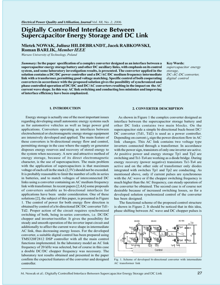
Electrical Power Quality and Utilisation, Journal Vol. XII, No. 2, 2006 Digitally Controlled Interface Between Supercapacitor Energy Storage and DC Link Mietek NOWAK, Juliusz HILDEBRANDT, Jacek RABKOWSKI, Roman BARLIK, Member IEEE Warsaw University of Technology, Poland Summary: In the paper specification of a complex converter designed as an interface between a supercapacitor energy storage battery and other DC auxiliary links, with emphasis on its control system, and some laboratory investigation results, is presented. The converter applied in the solution contains a DC/DC power controller and a DC/AC/DC medium frequency intermediate link with a transformer, permitting good voltage matching. Specific control of both cooperating converters in accordance with the proposed solution gives the possibility of synchronized and phase controlled operation of DC/DC and DC/AC converters resulting in the impact on the AC current wave shape. In this way AC link switching and conducting loss minimize and improving of interface efficiency have been emphasized. Key Words: supercapacitor energy storage, DC-AC-DC converter, digital control 1. INTRODUCTION 2. CONVERTER DESCRIPTION Energy storage is actually one of the most important issues regarding developing small autonomic energy systems such as for automotive vehicles as well as large power grid applications. Converters operating as interfaces between electrochemical or electromagnetic energy storage equipment are intensively developed and applied. The main feature of these converters is bi-directional energy flow and control, permitting storage in the case where the supply or generator disposes energy reserves and recovery of stored energy to the system when necessary. A new and attractive method of energy storage, because of its direct electromagnetic character, is the use of supercapacitors. The main problem with the application of supercapacitors is that maximum voltage of each cell in the stack (2,5V) should not be exceeded. It is probably reasonable to limit the number of cells in series in batteries, and to match voltages of interconnected DC links using a converter containing an AC medium frequency link with transformer. In recent papers [2,4,6] some proposals of converters suitable as bi-directional interfaces for applications have been under consideration. One of these solutions [2], the subject of this paper, is presented in Figure 1. The control of power for both energy flow direction is obtained by control of a bi-directional DC/DC converter Td1Td2. Proper action of the circuit requires synchronized switching of both, being in-series converters, i.e. DC/DC chopper and inverter/rectifier. It gives the possibility for steady and smooth operation of the inverter input circuit and additionally to affect the current wave shape in intermediate AC link, thus decreasing energy losses. For the developed converter, a suitable digital control has been prepared using TMS320F2812 DSP controller with all the main control functions implemented. In the laboratory model an AC link frequency of 20 kHz was selected, but of course in this case a double DC/DC chopper frequency was necessary. The laboratory test results obtained and presented in the paper confirm the expected features of the converter and designed controller. As shown in Figure 1 the complex converter designed as interface between the supercapacitor storage battery and other DC links contains two main blocks. On the supercapacitor side a simple bi-directional buck-boost DC/ DC converter (Td1, Td2) is used as a power controller. Depending on current id sign the power direction flow in AC link changes. This AC link contains two voltage type inverters connected through a transformer. In accordance with the power sign, transistors of only one inverter are active. At positive power and energy storage Tp1 and Tp2 are switching and Ts1-Ts4 are working as a diode bridge. During energy recovery (power negative) transistors Ts1-Ts4 are active and on the other side of transformer only diodes integrated with switches Tp1 and Tp2 are conducting. As mentioned above, only if current pulses are synchronous with the AC wave or if the chopper switching frequency is much higher than the AC frequency, can steady operation of the converter be obtained. The second case is of course not desirable because of increased switching losses, so for a developed solution synchronized control of the converter has been designed. The functional scheme of the proposed control structure is shown in Figure 2. It should be noticed that in this idea, phase shifting between AC wave and DC chopper pulses is Fig. 1. Scheme of developed bi-directional converter with intermediate AC transformer link M. Nowak et al.: Digitally Controlled Interface Between Supercapacitor Energy Storage and DC Link % gives AC current wave-shape in transformer: i Lk (x − x k ) = I dk + (U pk − U Cik ) sin wr (x − x k ) + KKKK .... + ( I ik − I dk ) cos wr (x − x k ) (2) and voltage on the intermediate capacitor Cd: u Cdk (x − x k ) = U pk − (U pk − U Cik ) cos wr (x − x k )K Fig. 2. Functional scheme of control structure permitting for synchronous switching of DC/DC and DC/AC converters possible. For the analysis of AC current waveform in the transformer and both DC/AC and AC/DC converters a simple equivalent circuit as given in Fig.3a. is useful. Input capacitor Cd builts together with transformer stray inductance Ls is an oscillating circuit excited by current pulses delivered from the DC chopper. In each time interval during the whole halfperiod of the AC voltage wave, this same equation and its solution respectively of intermediate transformer current iL and its secondary voltage Udp can be used, taking into account changing current values in particular time intervals The solution of the differential equation ignoring the remeining resistance: Up − Xs di L − 1 (i L − I d )d x = 0 dx YC ∫ where: YC = Cd(wB2Ls); x = wB t (1) KKKKK + I ik sin wr (x − x k ) YC (3) where: k number of sequential interval, wr = (wr / wB) = 1 / sqrt (XsYC), UCik, Iik capacitor voltage and inductance current initial values on beginning of k-th interval. The complex solution of the above given equations of the whole half-period is rather complicated and an important parameter needs to be taken into account, i.e. phase shifting of current pulses provided to the AC link from the DC chopper. Simulations seemed in this case a quite reasonable method of solution. In Figure 3c an example bunch of curves representing the AC link current half-period waves is shown. As a parameter, a phase shifting angle y related to p is used. Another important set of parameters which have to be considered regarding current wave shape are the values of leakage inductance of the transformer and capacitance of Cd. By selecting the value of this capacitance to obtain a resonant frequency close to the switching frequency and matching the value of phase shifting depending on power value and sign, it is possible to minimize power losses in the AC link. Fig. 3. Converter equivalent circuit (a), typical AC current (is) and AC voltage waveforms(us) and dc-pulse current (id) (b) and diagrams of current waves depending of y and Yc (c) & Power Quality and Utilization, Journal Vol. XII, No 2, 2006 3. MICROPROCESSOR IMPLEMENTATION OF CONTROL According to the functional scheme of developed interface control (Fig. 2.) presented above, a TMS320F2812 DSPbased controller has been designed. Power control is related to storage capacitor voltage and is obtained through duty ratio D control of the bi-directional DC/DC converter. The value of commanded current is calculated taking into account the supercapacitor voltage. It is very important not to exceed the maximal acceptable value as determined by the limited value of supercapacitor cells. If the capacitor voltage reaches the permitted value the loading current must be set to zero. The switching frequency of the AC intermediate link is equal to half of the chopper switching frequency. Only transistors of one of both inverters that are coupled through transformer inverters must be switched at the same time always on the side which delivers energy. Transistors comprising the other side of the converter stay off, so this complementary inverter is working as a simple diode rectifier. In the control algorithm and hardware arrangement, matching of phase shifting y between chopper current pulses and AC voltage wave is connected with the dc- current value control parameter duty ratio D, obtained as the output of the PI- controller. These two quantities which define current pulse width (D) and its front edge position (y) have the same representation related to the AC-half-period and chopper switching period Ts. Execution of D and y settings is done using a controller built-in modulator with a complex function. Three programmable counters are necessary for generation of control signal patterns of chopper and inverters. The way by which this has to be achieved is explained with time diagrams in Figure 4. Both cases represented by diagrams a) and b) are differentiated using condition: D+y <1 or D+y >1 . The complete flow-chart of the developed control program is shown in Figure 5a, and in the Figure 5b the functional scheme of hardware with logical interface circuit is presented. Fig. 4. Time diagrams explaining modulator output pattern at two possible conditions: y + D < 1 (a) and y + D > 1 (b) 4. LABORATORY MODEL TESTS The careful investigation of a constructed 4,5 kW laboratory model of converters and its microprocessor control (Figure 6) have confirmed all expectations in accordance with the main features of the proposed solution. An especially effective method of affecting the current wave-shape in AC intermediate link has been proved. In Figure 7 appropriate records of current waves at three different DC converter current pulse phase shifting values are presented. It is noticeable that changing current waveform results also in significant changing of switching current values in AC/DC/ AC converters. This interesting property of the designed control shows the possibility of adaptive control of phase shifting. The curves in Figure 8 measured for different values of y and both power flow directions prove this thesis. An important part of the laboratory investigation concerned the dynamic properties of the current control loop. A set of records showing fast step response of digitally controlled current are given in Figure 9. Fig. 5. Flow chart of control algorithm (a) and scheme explaining mP interface for transistor drives Fig. 6. Photo of laboratory bunch converter model and its mP control board M. Nowak et al.: Digitally Controlled Interface Between Supercapacitor Energy Storage and DC Link ' a) a) b) b) Fig. 8. Diagrams of measurem efficiency of converter at different y values and storage (a) and recovery (b) process c) Fig. 7. AC circuit current (is) and voltage (us) registered at different y values: y = 18°el, (a), y = 54°el , (b), y = 126°el (c) 5. CONCLUSIONS For the proposed and laboratory constructed converter interface with a medium frequency intermediate link, a full digital control of power and current control has been successfully tested. Thanks to precise and controllable synchronizing of a DC/DC bi-directional converter with DC/ AC inverters, a possibility of AC current shaping and efficiency optimization has been demonstrated. The ! laboratory measurements have shown efficiency improvements of 25 percent. The DSP processor TMS320F2812 gives a possibility of complete implementation of speedy power control including energy flow reverse. Additionally, a method of energy optimization has been proved APPENDIX Basic laboratory stand parameters: UCS = 12,5 25 V Udp = 300V fs = 20 kHz /40 kHz Cd = 80 mF LS = 0.75 mH ACKNOWLEDGMENT The job is sponsored by Polish State Committee for Scientific Research (Project No. 4T10A 050 25) . Power Quality and Utilization, Journal Vol. XII, No 2, 2006 2. N o w a k M . , H i l d e b r a n d t J . , B a r l i k R . : Bidirectional Converters as Power Interfaces for Supercapacitor Energy Storage Applications. EDPE 2003 pp. 551. 3. N o w a k M . , H i l d e b r a n d t J . , £ u n i e w s k i P .: Converters with AC Transformer Intermediate Link Suitable as Interfaces for Supercapacitor Energy Storage. PESC 2004 pp. 4067. 4. D e D o n c k e r R . , D i v a n D . M . , K h e r a l u w a l a M . H .: A three phase soft switched, high power density dc-dc converter for high power applications. IEEE Trans Ind. Appl. 1991, 27. pp. 6373. 5. W a l t e r J . , D e D o n c k e r R . : High power bi-directional DC/DC Converter Topology For Future Automobiles. Conf. Rec. CD-ROM EPE 2003 Tolouse. 6. R u f e r A . : Power Electronic Interface For a SupercapacitorBased Energy Storage Substation in DC Transportation Networks. Conf. Rec. CD-ROM EPE 2003 Tolouse. 7. TMS320F2812 Users Manual. a) Mieczys³aw Nowak Assistant-professor in the Institute of Control and Industrial Electronics Warsaw University of Technology. His main interest field are converters for drive applications and power conditioning. As author and co-author published over 100 papers, also 28 patents and 6 books in power electronics and converter control. As research team leader he took part and realized about 50 R&D projects ( also as national grants) many of this direct for industry applications. Since 1996 is a head of University Promotion Centre in Power Electronics where he has organised many short courses and tutorials for industry. He spent about 3 years on West-European Universities (RWTH Aachen, TU Graz) and electrical companies (BBC/ABB- Swiss). Juliusz Hildebrandt was born in Warsaw, Poland in 1976. Graduated from WUT in 2001. He is currently a PhD-student in the Institute of Control and Industrial Electronics and now is finishing his PhD thesis . His main interest area is topology and control of bi-directional converters, and supercapacitor energy storage. b) Jacek Rabkowski received the MSc.and Ph.D. degrees from the Warsaw University of Technology in 2000 and 2005 respectively. He is currently a Assistant Professor in Electrical Engineering Faculty at the Warsaw University of Technology. He is author and c-author of over ten papers. His main interest area is power electronics converters for renewable energy sources and energy storage. Roman Barlik c) Fig. 9. Dynamic features of investigated converter with digital control: step current command at storage (input and output converter current) a) current command at recovery b) current reverse c) REFERENCES was born in Bydgoszcz, Poland, in 1947. He received the MSc., Ph.D. and Sc.D. degrees from the Warsaw University of Technology in 1972, 1977 and 1987 respectively. He is currently a Professor in Electrical Engineering Faculty at the Warsaw University of Technology. From 1999 to 2005 he was a Dean of this Faculty. In 1982/1983 he was a Guest Researcher with the Faculty of Electrical Engineering of the Aachen University of Technology, Germany. He has carried out research in the field of static converters, electrical drives and industrial automation and has authored and co-authored more than 150 papers, published in refereed international and domestic journals and conference proceedings. He is co-author of the Handbook of Power Electronics. He has directed numerous research projects granted by the University, industrial companies and State Research Committee. He holds 20 Poland patents. He is a Senior Member of the IEEE. 1. N o w a k M . , H i l d e b r a n d t J . , B a r l i k R . : Investigation of bi-directional converters with intermediate transformer link designed as interfaces for supercapacitor energy storage. in Polish ,Conf. Rec. Modeling and Simulation Zakopane 2004. M. Nowak et al.: Digitally Controlled Interface Between Supercapacitor Energy Storage and DC Link !
