HDLX-1414 Series
Four Character Smart Alphanumeric Displays
Data Sheet
Description
Features
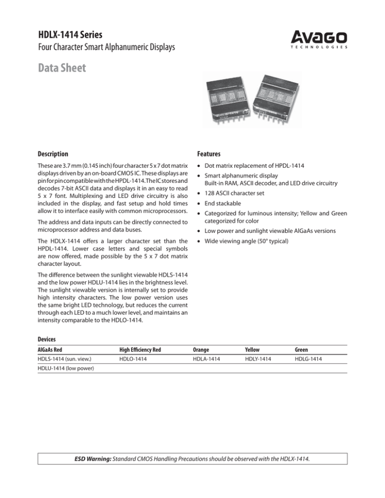
These are 3.7 mm (0.145 inch) four character 5 x 7 dot matrix
displays driven by an on-board CMOS IC. These displays are
pin for pin compatible with the HPDL-1414. The IC stores and
decodes 7-bit ASCII data and displays it in an easy to read
5 x 7 font. Multiplexing and LED drive circuitry is also
included in the display, and fast setup and hold times
allow it to interface easily with common microprocessors.
Dot matrix replacement of HPDL-1414
The address and data inputs can be directly connected to
microprocessor address and data buses.
The HDLX-1414 offers a larger character set than the
HPDL-1414. Lower case letters and special symbols
are now offered, made possible by the 5 x 7 dot matrix
character layout.
Smart alphanumeric display
Built-in RAM, ASCII decoder, and LED drive circuitry
128 ASCII character set
End stackable
Categorized for luminous intensity; Yellow and Green
categorized for color
Low power and sunlight viewable AlGaAs versions
Wide viewing angle (50° typical)
The difference between the sunlight viewable HDLS-1414
and the low power HDLU-1414 lies in the brightness level.
The sunlight viewable version is internally set to provide
high intensity characters. The low power version uses
the same bright LED technology, but reduces the current
through each LED to a much lower level, and maintains an
intensity comparable to the HDLO-1414.
Devices
AlGaAs Red
High Efficiency Red
Orange
Yellow
Green
HDLS-1414 (sun. view.)
HDLO-1414
HDLA-1414
HDLY-1414
HDLG-1414
HDLU-1414 (low power)
ESD Warning: Standard CMOS Handling Precautions should be observed with the HDLX-1414.
Package Dimensions
17.66
(0.695)
4.45 TYP.
(0.175)
0.25 ± 0.13 TYP.
(0.010 ± 0.005)
0.39 (2X) TYP.
(0.015)
15.30
(0.600)
9.14
(0.360)
20.12
(0.792)
PIN 1 IDENTIFIER
PART NUMBER
LUMINOUS INTENSITY
COLOR BIN [3]
DATE CODE (YEAR, WEEK)
HDLX-1414
6.10
(0.240)
YYWW
X
Z
PIN NO.
4.10
(0.160)
PIN 1
0.51 ± 0.13
(0.020 ± 0.005) TYP.
2.54 TYP.
(0.100)
FUNCTION
PIN NO.
FUNCTION
1
D5 DATA INPUT
7
2
D4 DATA INPUT
8
D0 DATA INPUT
3
WR WRITE
9
D1 DATA INPUT
4
A1 DIGIT SELECT
10
D2 DATA INPUT
5
A0 DIGIT SELECT
11
D3 DATA INPUT
6
VDD
12
D6 DATA INPUT
GROUND
DIMENSIONS ARE IN MILLIMETERS (INCHES).
Absolute Maximum Ratings
Parameter
Max.
Units
Supply Voltage, VDD to Ground[1]
Symbol
–0.5
Min.
Typ.
7.0
V
Input Voltage, Any Pin to Ground
–0.5
+0.5
V to VDD
Free Air Operating Temperature Range
TA
–40
+85
°C
Storage Temperature
TS
–40
+100
°C
+150
°C
CMOS IC Junction Temperature
Relative Humidity (Noncondensing) at +65°C
85%
Soldering Temperature, [1.59 mm (0.063 in.) Below Body]
Solder Dipping
Wave Soldering
260°C for 5 secs
250°C for 3 secs
ESD Classification, R = 1.5 k, C = 100 pF
Class 1 (0 – 1999 V)
Note:
1. Maximum Voltage is with no LEDs illuminated.
2
Character Set
ASCII
CODE
0
1
0
1
0
1
0
1
0
1
0
1
0
1
0
1
D1
0
0
1
1
0
0
1
1
0
0
1
1
0
0
1
1
D2
0
0
0
0
1
1
1
1
0
0
0
0
1
1
1
1
D3
0
0
0
0
0
0
0
0
1
1
1
1
1
1
1
1
0
1
2
3
4
5
6
7
8
9
A
B
C
D
E
F
D6
D5
D4
HEX
0
0
0
0
0
0
1
1
0
1
0
2
0
1
1
3
1
0
0
4
1
0
1
5
1
1
0
6
1
1
1
7
NOTES: 1 = HIGH LEVEL
0 = LOW LEVEL
3
D0
Recommended Operating Conditions
Parameter
Symbol
Min.
Typ.
Max.
Units
Supply Voltage
VDD
4.5
5.0
5.5
V
Electrical/Optical Characteristics over Operating Temperature Range
4.5 < VDD < 5.5 V (unless otherwise specified)
-25°C[1]
Parameter
Symbol
Blank Current
IDD (blnk)
Input Current
II
Input Voltage High
Input Voltage Low
IDD 4 Digits
20 dots/character[2,3]
IDD (#)
Min.
Typ.
Max.
Max.
Units
Test Conditions
4.0
mA
All Digits Blanked
–40
10
A
VIN = 0 V to VDD
VDD = 5.0 V
VIH
2.0
VDD
V
VIL
GND
0.8
V
160
mA
1.0
110
130
“#” ON in All Four Locations
Notes:
1. VDD = 5.0 V.
2. Average IDD measured at full brightness. Peak IDD = 28/15 x Average IDD (#).
3. IDD (#) max. = 130 mA, 150°C IC junction temperature and VDD = 5.5 V.
Optical Characteristics at 25°C[1]
VDD = 5.0 V at Full Brightness
AlGaAs Red HDLS-1414
Parameter
Symbol
Min.
Typ.
Units
Test Conditions
Average Luminous Intensity per Digit,
Character Average
IV
4.0
12.7
mcd
“*” Illuminated in All Four Digits.
19 Dots ON per Digit.
Peak Wavelength
PEAK
645
nm
Dominant Wavelength[2]
D
637
nm
AlGaAs Red HDLU-1414
Parameter
Symbol
Min.
Typ.
Units
Test Conditions
Average Luminous Intensity per Digit,
Character Average
IV
1.2
3.1
mcd
“*” Illuminated in All Four Digits.
19 Dots ON per Digit.
Peak Wavelength
PEAK
645
nm
Dominant Wavelength[2]
D
637
nm
4
High Efficiency Red HDLO-1414
Parameter
Symbol
Min.
Typ.
Units
Test Conditions
Average Luminous Intensity per Digit,
Character Average
IV
1.2
3.5
mcd
“*” illuminated in All Four Digits.
19 Dots ON per Digit.
Peak Wavelength
PEAK
635
nm
Dominant Wavelength[2]
D
626
nm
Orange HDLA-1414
Parameter
Symbol
Min.
Typ.
Units
Test Conditions
Average Luminous Intensity per Digit,
Character Average
IV
1.2
3.5
mcd
“*” Illuminated in All Four Digits.
19 Dots ON per Digit.
Peak Wavelength
PEAK
600
nm
Dominant Wavelength[2]
D
602
nm
Yellow HDLY-1414
Parameter
Symbol
Min.
Typ.
Units
Test Conditions
Average Luminous Intensity per Digit,
Character Average
IV
1.2
3.7
mcd
“*” Illuminated in All Four Digits.
19 Dots ON per Digit.
Peak Wavelength
PEAK
583
nm
Dominant Wavelength[2]
D
585
nm
Green HDLG-1414
Parameter
Symbol
Min.
Typ.
Units
Test Conditions
Average Luminous Intensity per Digit,
Character Average
IV
1.2
5.6
mcd
“*” Illuminated in All Four Digits.
19 Dots ON per Digit.
Peak Wavelength
PEAK
568
nm
Dominant Wavelength[2]
D
574
nm
Notes:
1. Refers to the initial case temperature of the device immediately prior to the light measurement.
2. Dominant wavelength, D, is derived from the CIE chromaticity diagram, and represents the single wavelength which defines the color of the
device.
5
AC Timing Characteristics over Operating Temperature Range at VDD = 4.5 V
Parameter
Symbol
Min.
Units
Address Setup
tAS
10
ns
Address Hold
tAH
40
ns
Data Setup
tDS
50
ns
Data Hold
tDH
40
ns
Write Time
tW
75
ns
Timing Diagram
Enlarged Character Font
2.29 (0.090)
TYP.
2.0 V
A0 – A1
0.8 V
tAS
0.56 (0.022)
TYP.
tAH
2.0 V
WR
0.8 V
3.61 (0.142)
TYP.
tW
2.0 V
D0 – D6
0.8 V
tDS
tDH
0.25 (0.010)
TYP.
0.51 (0.020)
TYP.
NOTES:
1. UNLESS OTHERWISE SPECIFIED, THE TOLERANCE ON
ALL DIMENSIONS IS ± 0.254 mm (0.010").
2. DIMENSIONS ARE IN MILLIMETERS (INCHES).
6
Electrical Description
Pin Function
Description
\Write (\WR, Pin 3)
WR must be logic 0 to store data in the display.
Address Inputs
(A1 and A0, Pins 4 and 5)
A0 and A1 select a specific location in the display memory. Address 00 accesses the far right
character, and address 11 accesses the far left position.
VDD (Pin 6)
VDD is the positive power supply input.
Ground (GND, Pin 7)
Ground is the display ground.
Data Inputs
(D0–D6, Pins 1, 2, 8-12)
D0–D6 are used to specify the input data for the display.
Display Internal Block Diagram
Figure 2 shows the HDLX-1414 display internal block
diagram. The CMOS IC consists of a 4 x 7 Character RAM,
a 128-character ASCII decoder and the refresh circuitry
necessary to synchronize the decoding and driving of four
5 x 7 dot matrix characters.
Four 7-bit ASCII words are stored in the Character RAM.
The IC reads the ASCII data and decodes it vita the
128-character ASCII decoder. This decoder includes the
64-character set of the HPDL-1414, 32 lower case ASCII
symbols, and 32 foreign language symbols.
Data Entry
Figure 1 shows a truth table for the HDLX-1414 display.
Address inputs A0 and A1 are used to select the digit
location in the display. When A0 and A1 are both logic low,
data is loaded into the right most character.
Data inputs D0–D6 are used to load information into the
display. Data is latched into the given character address on
the rising edge of the \WR signal. Data and Address inputs
must be held stable during the write cycle to ensure that
correct data is stored in the display.
Mechanical and Electrical Considerations
The HDLX-1414 is a 12-pin DIP package that can be
stacked to create a character array of any size. The display
is designed to operate reliably in –40˚C to +85˚C ambient
temperatures.
ESD and Latchup Protection
The inputs to the CMOS IC are protected against static
discharge and input current latchup. However, for best
results, standard CMOS handling precautions should be
used. Prior to use, the HDLX-1414 should be stored in
antistatic tubes or conductive material. During assembly
a grounded conductive work area should be used, and
assembly personnel should wear conductive wrist straps.
Lab coats made of synthetic material should be avoided
since they are prone to static charge build-up. Input
current latchup can be caused when the CMOS inputs are
subjected either to a voltage below ground (Vin < ground)
or higher than VDD (Vin > VDD) and when a high current is
forced into the input. To prevent input current latchup and
ESD damage, unused inputs should be connected either
to ground or to VDD. Voltages should not be applied to the
inputs until VDD has been turned on, and high transient
input voltages should be eliminated.
\WR
A1
A0
D6
D5
D4
D3
D2
D1
D0
Function
1
X
X
X
X
X
X
X
X
X
No Change
0
0
0
Digit 0 ASCII Data (Right Most Character)
0
0
1
Digit 1 ASCII Data
0
1
0
Digit 2 ASCII Data
0
1
1
Digit 3 ASCII Data (Left Most Character)
0 = Logic 0; 1 = Logic 1; X = Do Not Care.
Figure 1. Display truth table.
7
The HDLX-1414 is assembled by die attaching and wire
bonding 140 LEDs and a CMOS IC to a high temperature printed circuit board. A polycarbonate lens is placed
over the PC board, creating a protective air gap over the
LED wire bonds. Backfill epoxy environmentally seals the
display package. This package construction makes the
display highly tolerant to temperature cycling and allows
wave soldering.
Write to
Character
RAM
CHARACTER RAM
A0 – A 1
D0 – D 6
2
7
WRITE
ADDRESS
ASCII DECODER
DATA
OUT
7
CHARACTER
SELECT
COLUMN
DATA
DATA IN
5
WRITE
WR
(4 x 7)
3 ROW
SELECT
COLUMN
DRIVERS
ROW
DRIVERS
OSC
+ 32
+7
ROW
SELECT
DISPLAY
Figure 2. Display internal block diagram.
Soldering Instructions
Contrast Enhancement
The HDLX-1414 is compatible with hand- and wave-solder
processes. The use of a no-clean flux is recommended.
The objective of contrast enhancement is to provide good
readability in the end user’s ambient lighting conditions.
By using both luminance (brightness) and chrominance
(color) contrast techniques, the ON dots of the display can
be made to stand out against a dark background.
The polycarbonate lens on these displays is incompatible
with some fluxes and cleaning solutions. It is not recommended for use with heated Terpene, or solutions
of propylene glycol monomethyl ether and monoethanolamine.
For further information on soldering and post-solder
cleaning, see Application Note 1027, Soldering LED
Components.
8
For further information on contrast enhancement, see
Application Note 1015, Contrast Enhancement Techniques
for LED Displays.
Color Bin Limits
Intensity Bin Limits for HDLS-1414
Color Range (nm)
Intensity Range (mcd)
Bin
Min.
Max.
Color
Bin
Min.
Max.
E
3.97
6.79
Green
1
576.0
580.0
F
5.55
9.50
2
573.0
577.0
G
7.78
13.30
3
570.0
574.0
H
10.88
18.62
4
567.0
571.5
I
15.24
26.07
3
581.5
585.0
J
21.33
36.49
4
584.0
587.5
5
586.5
590.0
6
589.0
592.5
Yellow
Note:
Test conditions as specified in Optical Characteristic table.
Note:
Test conditions as specified in Optical Characteristic table.
Intensity Bin Limits for HDLX-1414
Intensity Range (mcd)
Bin
Min.
Max.
A
1.20
1.77
B
1.45
2.47
C
2.02
3.46
D
2.83
4.85
E
3.97
6.79
F
5.55
9.50
G
7.78
13.30
Note:
Test conditions as specified in Optical Characteristic table.
For product information and a complete list of distributors, please go to our web site:
www.avagotech.com
Avago, Avago Technologies, and the A logo are trademarks of Avago Technologies in the United States and other countries.
Data subject to change. Copyright © 2005-2012 Avago Technologies. All rights reserved. Obsoletes 5989-3191EN
AV02-3611EN - June 12, 2012
