KSR-201 High Performance DC Solid State Relay /
Power Controller for Loads up to 2.5A @ 60Vdc
Product Facts
■ Combines isolated load
switching and circuit
protection capabilities.
■ Fast acting bounce-free
switching
■ Carries full rated load
(2.5A) without heat sinking
to 90°C.
■ Low output on-resistance
and voltage drop.
■ Meets surge requirement of
MIL-STD-1275 and MILSTD-740A.
■ Nuclear tolerance tested.
This controller features state
of the art photo-voltaic
optical input/output isolation
and power MOSFET output
switching technology for
reliable control of DC loads
up to 2.5 amps up to 90°C
ambient. Temperature
compensated output current
monitoring and trip circuitry
provide overload/short
circuit protection while
providing inrush current
handling capability for lamp,
motor, and inductive loads.
The output MOSFET chip is
rated at 100V to withstand
the abnormal power surge
requirements of MIL-STD1275 and MIL-STD-740A for
28Vdc systems. Thick film
hybrid construction is
employed in a low profile,
hermetically sealed package
that is designed and
screened to applicable
requirements of MIL-PRF28750D, Y level.
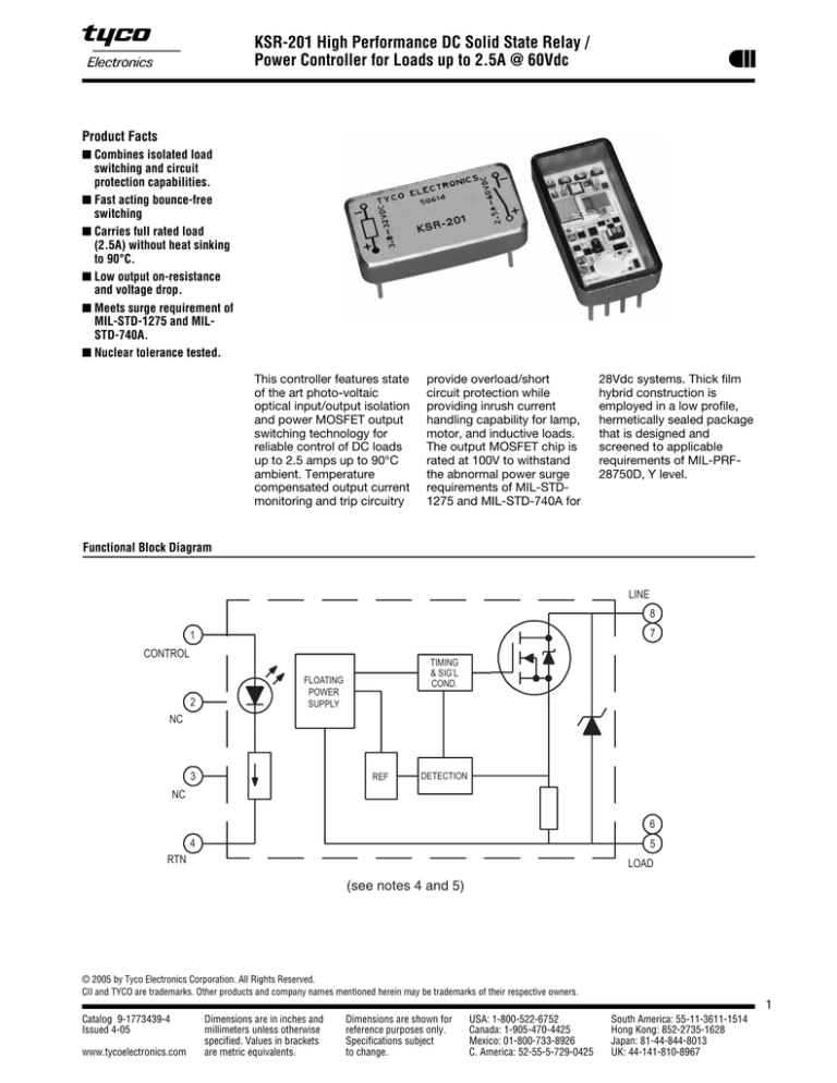
Functional Block Diagram
LINE
8
7
1
CONTROL
2
TIMING
& SIG’L
COND.
FLOATING
POWER
SUPPLY
NC
3
REF
DETECTION
NC
6
4
5
RTN
LOAD
(see notes 4 and 5)
© 2005 by Tyco Electronics Corporation. All Rights Reserved.
CII and TYCO are trademarks. Other products and company names mentioned herein may be trademarks of their respective owners.
1
Catalog 9-1773439-4
Issued 4-05
www.tycoelectronics.com
Dimensions are in inches and
millimeters unless otherwise
specified. Values in brackets
are metric equivalents.
Dimensions are shown for
reference purposes only.
Specifications subject
to change.
USA: 1-800-522-6752
Canada: 1-905-470-4425
Mexico: 01-800-733-8926
C. America: 52-55-5-729-0425
South America: 55-11-3611-1514
Hong Kong: 852-2735-1628
Japan: 81-44-844-8013
UK: 44-141-810-8967
High Performance Electronic Products
KSR-201 DC Solid State Relay / Power Controller (Continued)
Environmental Characteristics
Electrical Specifications (-55°C to +105°C unless otherwise specified)
Ambient Temperature Range:
Operating: -55°C to +105°C.
Storage: -55°C to +125°C.
Input
Vibration Resistance:
20 G’s, 10-2,000 Hz.
Control voltage range (Vcc)
Control current (max.) @ 5Vdc
3.8 - 32 Vdc (Notes 1 & 2, Figures 1 & 2)
15mAdc (Notes 1 & 2, Figures 1 & 2)
Must turn-on voltage
2.4Vdc
Shock Resistance:
1,500 G’s, 0.5 ms pulse.
Must turn-off voltage
1.5Vdc
Reverse voltage protection
-7Vdc
Constant Acceleration Resistance
(Y1 axis):
5,000 G’s.
I/O
Dielectric Strength (min.)
500V rms
Insulation Resistance (min.) @ 500Vdc
108 ohms
Output
Continuous load current (max.)
2.5Adc (Figure 4)
Mechanical Characteristics
Continuous load voltage (max.)
Weight (max.):
.35 oz. (10 grams)
Transient blocking voltage (max.)
On resistance (max.) @ IL = 100mA, 25°C
0.14 ohm
Materials:
Case: 1010 CRS, nickel plated
Pins: Copper cored Alloy 52, gold
plated
Output voltage drop (max.)
0.42Vdc
60Vdc
80Vdc (Note 2)
Leakage current (max.) @ V = 32Vdc
40µAdc
Turn-on time (max.)
1.8 ms (Note 3, Figure 5)
Turn-off time (max.)
1.1 ms (Figure 5)
Electrical system spike
600Vdc (Note 8)
Junction temperature (max.)
125°C
Thermal resistance (max.), junction to ambient
35°C/W
Thermal resistance (max.), junction to case
15°C/W
Inrush current, 75ms, no trip
10Adc (Figure 3)
Inrush current, 100ms, must trip
22Adc (Figure 3)
Inrush current, 200ms, no trip
4.5Adc (Figure 3)
Inrush current, 200ms, must trip
10Adc (Figure 3)
2
Catalog 9-1773439-4
Issued 4-05
www.tycoelectronics.com
Dimensions are in inches and
millimeters unless otherwise
specified. Values in brackets
are metric equivalents.
Dimensions are shown for
reference purposes only.
Specifications subject
to change.
USA: 1-800-522-6752
Canada: 1-905-470-4425
Mexico: 01-800-733-8926
C. America: 52-55-5-729-0425
South America: 55-11-3611-1514
Hong Kong: 852-2735-1628
Japan: 81-44-844-8013
UK: 44-141-810-8967
High Performance Electronic Products
KSR-201 DC Solid State Relay / Power Controller (Continued)
Figure 2 - Series Resistance vs. Vcc Input Voltage (Note 1)
20.0
2000
18.0
1800
16.0
1600
Series Resistance (ohms)
Input Current (mA)
Figure 1 - Input Current vs. Input Voltage
14.0
12.0
10.0
8.0
6.0
4.0
1400
1200
1000
800
600
400
2.0
200
0
0
0
2
4
6
8
10 12
0
28 30 32
3
0.01
12
15
18
21
24
27
Figure 4 - Thermal Derating
% Rated Load Current
% of Maximum Load Current
Figure 3 - Overload Trip Curve
0.001
9
Input Voltage (Vcc)
Input Voltage (Vcc)
32.5
30
27.5
25
22.5 Indeterminate
20
17.5
15
12.5
10
Must Not Trip
7.5
5
2.5
0
6
Must Trip
100%
-55
0
+25
+90 +105
Case Temperature (°C)
0.1
1
10
100
Trip Time (Seconds)
3
Catalog 9-1773439-4
Issued 4-05
www.tycoelectronics.com
Dimensions are in inches and
millimeters unless otherwise
specified. Values in brackets
are metric equivalents.
Dimensions are shown for
reference purposes only.
Specifications subject
to change.
USA: 1-800-522-6752
Canada: 1-905-470-4425
Mexico: 01-800-733-8926
C. America: 52-55-5-729-0425
South America: 55-11-3611-1514
Hong Kong: 852-2735-1628
Japan: 81-44-844-8013
UK: 44-141-810-8967
High Performance Electronic Products
KSR-201 DC Solid State Relay / Power Controller (Continued)
Figure 5 - Turn-On and Turn-Off Timing
HIGH
PIN 4 REF
TO 1
LOW
OFF
90%
PIN 8 TO 6
10%
T (on)
ON
T (off)
Figure 6 - Outline Dimensions
0.100
(2.54)
0.100
(2.54)
0.240 MAX.
(6.0)
0.500 MAX.
(12.7)
0.030 Ø
(0.75)
0.104
(2.51)
0.792
(20.11)
1.000 MAX.
(25.4)
TOLERANCES:
± 0.010 (0.25mm) FOR 2 PLACE DECIMALS;
± 0.005 (0.13mm) FOR 3 PLACE DECIMALS;
UNLESS OTHERWISE NOTED.
0.300
(7.62)
0.256 MAX.
(6.5)
Notes
1.For control voltages >6.0 Vdc, a series resistor is recommended. See Fig. 2 for value. The control voltage is the voltage across the input terminals (pin 1 referenced
to pin 4). Transition of the control voltage should be <1.0 msec and should be of a “bounce free” nature.
2.Tested to the requirements of MIL-STD-1275. For transients >80 Vdc, the power controller will be protected and will pass the current resulting from the transient on
to the load. The magnitude of the current is a function of the clamping voltage of the power controller and the source impedance of the transient. The clamping
voltage of the power controller is 100 Vdc ±5% with a temperature coefficient of 0.1%/°C.
3.Timing measurements taken with a resistive load, at VBIAS = 5.5 Vdc and measured between the 10% and 90% points.
4.The output of the Solid State Power Controller is floating, thereby allowing the load to be connected to the high or low side of the switch. The switch is capable of
sinking or sourcing the load current. Reversing the polarity of the line voltage may cause permanent damage.
5.Inductive loads must be diode suppressed. When switching into a shorted condition, series inductance must be <50 millihenries. Input repetition rate not to exceed
10 Hz when switching into a shorted condition.
6.To reset power controller after a shorted or overload condition has occurred, remove the short circuit or overload condition; then remove and reapply the control
voltage after a minimum 50 ms reset time.
7.The rated input voltage for functional tests shall be 5.0 Vdc. This includes tests for on-resistance, output voltage drop, timing, short circuit and overload protection.
8.Electrical system spike per MIL-PRF-28750, 10 ms
4
9-1773439-4–PDF–KRG–4-05
Printed in the U.S.A.
www.tycoelectronics.com
Dimensions are in inches and
millimeters unless otherwise
specified. Values in brackets
are metric equivalents.
Dimensions are shown for
reference purposes only.
Specifications subject
to change.
USA: 1-800-522-6752
Canada: 1-905-470-4425
Mexico: 01-800-733-8926
C. America: 52-55-5-729-0425
South America: 55-11-3611-1514
Hong Kong: 852-2735-1628
Japan: 81-44-844-8013
UK: 44-141-810-8967


