AN319
APPLICATION NOTE
RELAY DRIVE PROTECTION
INTRODUCTION
A fast switch-off in an inductive circuit causes overvoltages and electromagnetic interferences that can
damage peripheral elements. When a relay drive circuit is not protected, it is frequent to find some contacts destroyed by the arc due to the overvoltage or failed transistors after initial use. Various solutions
exist which limit the voltage at the terminals of the switching circuit in order to prevent any damage.
There follow some examples.
PASSIVE COMPONENTS
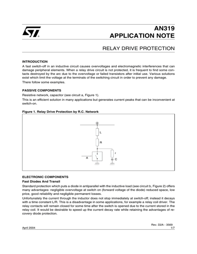
Resistive network, capacitor (see circuit a, Figure 1).
This is an efficient solution in many applications but generates current peaks that can be inconvenient at
switch-on.
Figure 1. Relay Drive Protection by R.C. Network
a
L
R
r
A
C
ELECTRONIC COMPONENTS
Fast Diodes And Transil
Standard protection which puts a diode in antiparallel with the inductive load (see circuit b, Figure 2) offers
many advantages: negligible overvoltage at switch on (forward voltage of the diode) reduced space, low
price, good reliability and negligible permanent losses.
Unfortunately the current through the inductor does not stop immediately at switch-off; instead it decays
with a time constant L/R. This is a disadvantage in some applications, for example a relay coil driver. The
relay contacts will remain closed for some time after the switch is opened due to the current stored in the
relay coil. It would be desirable to speed up the current decay rate while retaining the advantages of recovery diode protection.
April 2004
Rev. D2A - 3569
1/7
AN319 APPLICATION NOTE
A solution is shown in Figure 2, circuit c, in which a Transil diode is put in series with the recovery device.
A much higher voltage is developed across the diode-Transil combination than across a single diode, thus
accelerating the current decay.
Figure 2. Relay Drive Protection
c
b
L
L
D
R
T
D
R
A
A
Note: (b) Recovery Diode.
(c) Diode and Transil.
Transil
The Transil is an avalanche diode specially designed to clamp overvoltages and dissipate power in impulsive mode. It also offers the possibility of considerable average power absorption. It is available in different
cases covering a wide range of voltages (5 to 600V).
Moreover, all the necessary data to calculate power parameters and to carry out temperature evaluation
(Zth, Rth, etc...) can be found in technical notes. So the Transil is perfectly suited to this application.
In the case of a steady state power supply we can consider three hypotheses:
Circuit d (Figure 3). This is an economic solution which requires a unidirectional Transil only, but the current released by the inductance goes through the power supply and may affect the ground points.
Circuit c (Figure 2) and circuit e (Figure 3). The inductive discharge current only goes through the
LRD loop, thus is does not create disturbances in the ground points. This is a more expensive solution
since two diodes or one bidirectional Transil are necessary. In the case of an alternating sinusoidal supply
for low power, circuits e and f (Figure 3) are well suited to limit inductive overvoltages.
Comparison of the Current Decay Time in the Inductive Load Between the Recovery Diode and the
Transil Diode Schematics (see Figure 4)
The ratio t2/t1 represents the reduction in current decay time when a Transil is used.
1
t 2 ⁄ t 1 = -----------------------------------------------1 + 1, 4 ⋅ V CL ⁄ V CC
2/7
AN319 APPLICATION NOTE
Figure 3. Relay Drive Protection
e
d
f
L
L
L
I
R
R
R
I
A
A
A
T
Note: (d) Unidirectional Transil.
(e) Bidirectional Transil.
(f) Bidirectional Transil.
VCL is the voltage (measured) at the terminals of the Transil when the load current goes through it.
If we take VCL = VCC, we limit the overvoltage to a reasonable value and thus period t2 represents only
0.4 x t1. A correct choice of VCL will reduce t2 to very low values and reach the mechanical limit given by
the relay.
Figure 4. Current in the inductance at switch off
g
VCC
VCC
R
L
D
t1 = L Ln 2
R
VCC
2R
R
A
t1
t
VCC
R
h
VCC
L
VCC
2R
R
A
T
VCL
R
t2
t
Note: (g) Recovery diode circuit: current slowly decreases to 0.
(h) Transil circuit: current decreases rapidly (asymptote = –VCL* / R).
3/7
AN319 APPLICATION NOTE
CONCLUSION
The Transil is a must in relay drive circuits. It guarantees a reliable and efficient protection while reducing
the delay between the coil drive turn-off and the contact release.
EXAMPLE OF APPLICATION: CALCULATION AND CHOICE OF A TRANSIL
We wish to protect the transistor in Figure 5 by a Transil whose clamping voltage must not under any circumstances exceed VCL = 85V The clamping voltage is given by:
VCL = VBR + Rd IC
In the case of repetitive overload, the current is small enough such that the Rd Ic term can be neglected.
Thus VCL approximates to:
VCL = VBR
The calculation is therefore simplified, and the Transil can be selected according to its thermal resistance.
Mean Power Determination: PAV
A rough value can be obtained by assuming that all the energy contained in the inductance is absorbed
by the Transil.
This is true when VBR >> VCC.
12 + 24 2
1
1
2
P AV = --- ⋅ LI ⋅ f = --- ⋅ 035 ⋅ ------------------ ⋅ 50 = 09W
45
2
2
Stand Off Voltage Selection
The supply voltage varies between 9.6V and 14.4V.
The stand off voltage of the diode VRM will be
therefore be greater than or equal to 14.4V.
VCL Determination
From the data sheets we can see that for a low
current, VCL = VBR.
Tj Calculation
Tj = Tamb + PAV x Rth = 50 + 90 = 140°C < Tj max (150°C)
This value is consistent with the characteristics of the BZW04- 61B Transil (F 126 case) but the safety
margin is somewhat low, so a device from the 1500 W series is preferable as a first choice.
{ 1.5 KE 75CP (CB– 429 case): VBR max = 82.5V, Rth = 75°C/W, VRM = 64.1V > 14.4V
Tj = 50 + 68 = 118°C Tj max = 175°C
Temperature Correction
Voltage at 118°C is:
VCL (118°C) = VCL (25°C) [1 + αT (118 - 25)] = [1 + 10.5 x 10⁻⁴ (93)] 82.5 = 90.5V
This value is too high.
Definitive Choice
1.5 KE 68CP: VBR max = 74.8V, VRM = 58.1V > 14.4V
⇒ 1.5 KE 68CP is suitable.
4/7
VCL (118°C) = 1.098 x 74.8 = 82.5V
AN319 APPLICATION NOTE
Figure 5. Schematic of the Example
VCC
12 V ± 20%
L = 0.35 H
T
R = 45 Ω
Repetitive
f = 50 Hz
Tamb max 50˚C
5/7
AN319 APPLICATION NOTE
REVISION HISTORY
Table 1. Revision History
6/7
Date
Revision
Description of Changes
March-1993
1
First Issue
16-Apr-2004
2
Stylesheet update. No content change.
AN319 APPLICATION NOTE
Information furnished is believed to be accurate and reliable. However, STMicroelectronics assumes no responsibility for the consequences
of use of such information nor for any infringement of patents or other rights of third parties which may result from its use. No license is granted
by implication or otherwise under any patent or patent rights of STMicroelectronics. Specifications mentioned in this publication are subject
to change without notice. This publication supersedes and replaces all information previously supplied. STMicroelectronics products are not
authorized for use as critical components in life support devices or systems without express written approval of STMicroelectronics.
The ST logo is a registered trademark of STMicroelectronics.
All other names are the property of their respective owners
© 2004 STMicroelectronics - All rights reserved
STMicroelectronics GROUP OF COMPANIES
Australia - Belgium - Brazil - Canada - China - Czech Republic - Finland - France - Germany - Hong Kong - India - Israel - Italy - Japan Malaysia - Malta - Morocco - Singapore - Spain - Sweden - Switzerland - United Kingdom - United States
www.st.com
7/7

