Avago MGA-68563-BLKG datasheet: pdf
advertisement
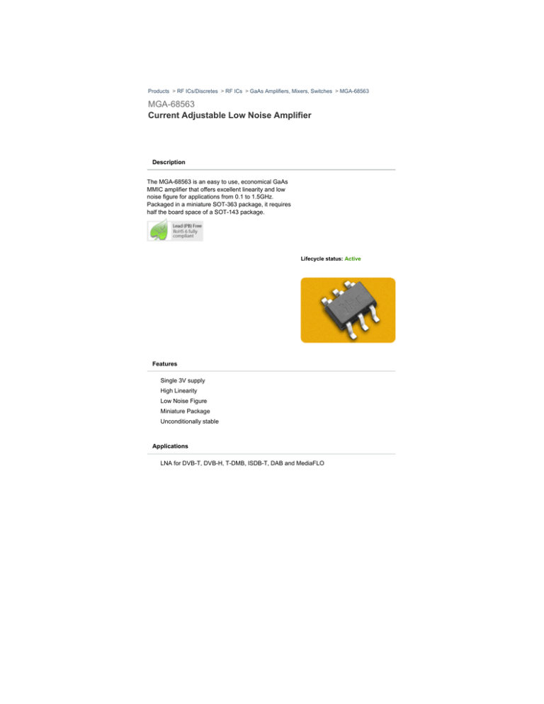
Products > RF ICs/Discretes > RF ICs > GaAs Amplifiers, Mixers, Switches > MGA-68563 MGA-68563 Current Adjustable Low Noise Amplifier Description The MGA-68563 is an easy to use, economical GaAs MMIC amplifier that offers excellent linearity and low noise figure for applications from 0.1 to 1.5GHz. Packaged in a miniature SOT-363 package, it requires half the board space of a SOT-143 package. Lifecycle status: Active Features Single 3V supply High Linearity Low Noise Figure Miniature Package Unconditionally stable Applications LNA for DVB-T, DVB-H, T-DMB, ISDB-T, DAB and MediaFLO MGA-68563 Current-Adjustable, Low Noise Amplifier Data Sheet Description Features Avago Technologies MGA-68563 is an economical, easyto-use GaAs MMIC amplifier that offers excellent linearity and low noise figure for applications from 0.1 to 1.5 GHz. Packaged in an miniature SOT-363 package, it requires half the board space of a SOT-143 package. • Single +3V supply One external resistor is used to set the bias current from 5mA to 30mA. This allows the designer to use the same part in several circuit positions and tailor the linearity performance (and current consumption) to suit each position. • Unconditionally stable The output of the amplifier is matched to 50Ω (below 2:1 VSWR) across the entire bandwidth and only requires minimum input matching. The amplifier allows a wide dynamic range by offering a 1.0 dB NF coupled with a +20 dBm Output IP3. The circuit uses state-of-the-art E‑pHEMT technology with proven reliability. On-chip bias circuitry allows operation from a single +3V power supply, while internal feedback ensures stability (K>1) over all frequencies for Id at 10mA and above. Applications • LNA for DVB-T,DVB-H, T-DMB, ISDB-T, DAB and MediaFLO • High linearity • Low noise figure • Miniature package Specifications at 500 MHz; 3V, 10 mA (Typ.) • 1.0 dB noise figure • 20 dBm OIP3 • 19.7 dB gain * This represents what Avago Technologies has managed to achieve on a device level with trade off between optimal NF, Gain, OIP3 and input return loss. Attention: Observe precautions for handling electrostatic sensitive devices. ESD Machine Model (Class A) ESD Human Body Model (CLass 1A) Refer to Agilent Application Note A004R: Electrostatic Discharge Damage and Control. Pin Connections and Package Marking Simplified Schematic Vd Ibias OUTPUT 6 and V d GND 1 INPUT 3 6Cx GND 2 5 GND 4 BIAS Id = Ids + Ibias Rbias Note: Package marking provides orientation and identification: Ids Feedback Vbias 4 “6C” = Device Code “x” = Date code indicates the month of manufacture. Input match RFin 6 RFout 3 Bias 1, 2, 5 GND MGA-68563 Absolute Maximum Ratings[1] Symbol Parameter Units Absolute Maximum Vd Device Voltage (pin 6) [2] V 6 Id Device Current (pin 6) [2] mA 100 Pin CW RF Input (pin3) (Vd=3V, Id=10mA) [3] (Vd=0V, Id=0mA) dBm dBm 21 21 Iref Bias Reference Current (pin 4) mA 1 Pdiss Total Power Dissipation [4] mW 600 TCH Channel Temperature °C 150 TSTG Storage Temperature °C 150 θch_b Thermal Resistance [5] °C/W 97 + Wire Supplying Vbias from Agilent 4142 10 nF 3V _ Notes: 1. Operation of this device above any one of these parameters may cause permanent damage. 2. Bias is assumed at DC quiescent conditions. 3. With the DC (typical bias) and RF applied to the device at board temperature TB = 25°C. 4. Total dissipation power is referred to lead “5” temperature. Tc=92°C, derate Pdiss at 10.3mW/°C for Tc>92°C. 5. Thermal resistance measured using 150°C Liquid Crystal Measurement method. 47 nH 4300 Ω 6Cx 68 pF Blocking Cap Direct to Direct to Ground Ground 4 6.8 nH 100 pF 3 MGA-68563 RF Output 6 Bias Bias Tee 100 pF 1 2 5 Figure 1a. Test circuit of the 0.5 GHz production test board used for NF, Gain and OIP3 measurements. This circuit achieves a trade-off between optimal NF, Gain, OIP3 and input return loss. Circuit losses have been de-embedded from actual measurements. RF Input Vdd supply from Agilent 4142 Reference Planes Figure 1b. A diagram showing the connection to the DUT during an S and Noise parameter measurement using an automated tuner system. MGA-68563 Electrical Specifications TC = 25°C, ZO = 50Ω, Vd = 3V (unless otherwise specified) Symbol Parameters and Test Conditions Freq Units Min. Typ. Max. Id [1,2] Device Current mA 11 16 NFtest [1,2] Noise Figure in test circuit [1] f = 0.5 GHz dB 1.0 1.4 Gtest [1,2] Associated Gain in test circuit [1] f = 0.5 GHz dB 18 19.7 21.5 f = 0.5 GHz dBm 18 20.7 OIP3test [1,2] Output 3rd Order Intercept in test circuit [1] P1dBtest [1,2] Output Power at 1dB Gain Compression in test circuit. [1] f = 0.5 GHz dBm17.5 Notes: 1. Guaranteed specifications are 100% tested in the production test circuit, the typical value is based on measurement of at least 600 parts from two non-consecutive wafer lots during initial characterization of this product. 2. Circuit achieved a trade-off between optimal NF, Gain, OIP3 and input return loss. LSL USL LSL CPK=2.13 CPK=3.228 6 7 8 9 10 11 12 13 14 15 16 17 Figure 2. Id @ 3V.LSL=7, Nominal=11, USL=16 19 20 21 22 Figure 3, OIP3 @ 0.5GHz 3V. LSL=18, Nominal=20.7 USL CPK=1.62 18 LSL USL CPK=2.276 .7 .8 .9 1 1.1 1.2 1.3 1.4 1.5 Figure 4. NF @ 0.5GHz 3V.USL=1.4, Nominal=1.0 18 18.5 19 19.5 20 20.5 21 21.5 22 Figure 5. Gain @ 0.5GHz 3V.USL=18, Nominal=19.7, USL=21.5 Note: Measured on the production circuit. Distribution data sample size is 600 samples taken from 2 non-consecutive wafer lots. Future wafers allocated to this product may have nominal values anywhere between upper and lower limits. MGA-68563 Typical Scattering Parameters, Tc = 25°C, Zo = 50ohm, Vd = 3V, Ids = 10mA Freq. GHz Mag. S11 Ang. dB S21 Mag. Ang. Mag. S12 Ang. Mag. S22 Ang. K-factor 0.3 0.42 -37.10 19.26 9.18 158.40 0.07 5.40 0.27 -32.20 1.01 0.5 0.36 -57.20 18.81 8.72 145.00 0.07 3.80 0.19 -47.50 1.04 0.7 0.38 -76.30 18.16 8.09 133.90 0.07 3.90 0.19 -63.10 1.02 0.9 0.40 -92.50 17.43 7.44 123.90 0.07 4.10 0.18 -75.80 1.03 1.0 0.41 -99.70 17.07 7.14 119.30 0.07 4.10 0.17 -81.80 1.03 1.1 0.42 -106.70 16.70 6.84 115.00 0.07 4.20 0.17 -86.30 1.04 1.3 0.44 -119.50 16.00 6.31 106.80 0.07 4.40 0.16 -95.10 1.04 1.5 0.45 -132.30 15.36 5.86 99.40 0.07 4.50 0.17 -98.30 1.06 1.7 0.47 -141.10 14.71 5.44 92.30 0.07 4.60 0.16 -107.70 1.08 1.9 0.48 -150.50 14.09 5.06 85.60 0.08 4.60 0.15 -115.30 1.11 2.0 0.49 -154.60 13.81 4.90 82.50 0.08 4.60 0.15 -116.20 1.11 2.5 0.51 -176.40 12.46 4.20 67.00 0.08 3.10 0.14 -131.90 1.16 3.0 0.50 160.80 11.13 3.60 53.80 0.09 2.00 0.15 -153.10 1.28 3.5 0.50 142.70 10.13 3.21 41.80 0.09 0.30 0.15 -176.10 1.35 4.0 0.51 126.90 9.74 3.07 25.20 0.11 -8.60 0.08 162.40 1.29 Typical Noise Parameters at 25°C, Tc = 25°C, Zo = 50ohm, Vd = 3V, Ids = 10mA 13 Freq. GHz Fmin dB opt Mag. Ang. Rn/50 NF@50 dB 0.5 0.83 0.12 108.80 0.11 0.85 1.0 0.74 0.05 109.80 0.08 0.74 1.5 0.76 0.16 151.40 0.07 0.80 2.0 0.88 0.21 147.90 0.07 0.94 2.5 1.05 0.24 161.50 0.06 1.12 3.0 1.24 0.26 -173.10 0.09 1.31 G W MGA-68563 Typical Scattering Parameters, Tc = 25°C, Zo = 50ohm, Vd = 3V, Ids = 5mA Freq. GHz Mag. S11 Ang. dB S21 Mag. Ang. Mag. S12 Ang. Mag. S22 Ang. K-factor 0.3 0.54 -28.80 16.61 6.77 160.50 0.07 6.50 0.43 -24.60 1.01 0.5 0.47 -44.40 16.31 6.54 147.20 0.08 4.20 0.35 -36.80 1.02 0.7 0.48 -60.80 15.77 6.15 136.80 0.08 4.00 0.33 -49.10 1.00 0.9 0.48 -75.60 15.15 5.72 127.10 0.08 3.60 0.31 -59.50 0.98 1.0 0.48 -82.30 14.85 5.53 122.60 0.08 3.10 0.30 -64.30 0.98 1.1 0.49 -89.20 14.53 5.33 118.40 0.08 2.80 0.29 -68.50 0.98 1.3 0.50 -102.00 13.93 4.97 110.30 0.09 2.00 0.28 -76.00 0.98 1.5 0.50 -114.50 13.37 4.66 102.90 0.09 1.10 0.28 -81.10 0.98 1.7 0.52 -124.30 12.82 4.38 95.80 0.09 0.10 0.25 -88.20 0.98 1.9 0.52 -134.20 12.27 4.11 88.90 0.09 -1.10 0.24 -94.80 1.01 2.0 0.53 -138.60 12.03 3.99 85.70 0.09 -1.50 0.23 -96.00 1.02 2.5 0.55 -162.10 10.86 3.49 69.70 0.10 -5.30 0.21 -110.40 1.07 3.0 0.53 173.50 9.61 3.02 55.60 0.10 -8.00 0.20 -127.80 1.23 3.5 0.51 153.90 8.67 2.71 42.90 0.10 -10.40 0.18 -146.80 1.35 4.0 0.53 137.40 8.38 2.62 26.70 0.11 -18.20 0.12 -153.40 1.32 Typical Noise Parameters at 25°C, Tc = 25°C, Zo = 50ohm, Vd = 3V, Ids = 5mA 14 Gopt Freq. GHz Fmin dB Mag. Ang. Rn/50 NF@50W dB 0.5 1.21 0.15 97.70 0.14 1.25 1.0 1.01 0.12 62.80 0.11 1.03 1.5 1.04 0.18 114.20 0.11 1.10 2.0 1.07 0.24 123.90 0.09 1.17 2.5 1.20 0.28 141.00 0.08 1.33 3.0 1.41 0.29 162.20 0.10 1.50 MGA-68563 Typical Scattering Parameters, Tc = 25°C, Zo = 50ohm, Vd = 3V, Ids = 15mA Freq. GHz Mag. S11 Ang. dB S21 Mag. Ang. Mag. S12 Ang. Mag. S22 Ang. K-factor 0.3 0.35 -43.60 20.54 10.64 157.30 0.06 5.00 0.18 -41.30 1.01 0.5 0.30 -67.40 19.99 9.99 143.70 0.06 3.90 0.11 -64.30 1.04 0.7 0.33 -87.40 19.27 9.20 132.40 0.06 4.40 0.12 -82.80 1.05 0.9 0.36 -103.80 18.49 8.41 122.20 0.06 5.30 0.12 -96.80 1.06 1.0 0.37 -110.90 18.10 8.03 117.60 0.06 5.60 0.12 -103.50 1.07 1.1 0.39 -117.60 17.70 7.68 113.20 0.06 6.10 0.12 -107.50 1.07 1.3 0.41 -129.90 16.95 7.04 105.00 0.06 7.10 0.12 -116.50 1.10 1.5 0.43 -142.10 16.26 6.50 97.60 0.06 7.90 0.12 -116.30 1.12 1.7 0.46 -150.20 15.57 6.00 90.70 0.07 8.60 0.12 -127.30 1.13 1.9 0.46 -159.10 14.91 5.56 84.00 0.07 9.10 0.12 -134.70 1.17 2.0 0.47 -162.90 14.61 5.38 81.00 0.07 9.30 0.11 -135.30 1.16 2.5 0.50 176.50 13.19 4.56 65.80 0.08 8.70 0.12 -149.80 1.20 3.0 0.50 154.70 11.82 3.90 53.00 0.08 7.90 0.14 -170.30 1.30 3.5 0.50 137.50 10.80 3.47 41.40 0.09 5.90 0.15 167.50 1.33 4.0 0.50 122.10 10.35 3.29 24.70 0.11 -3.90 0.09 137.50 1.27 Typical Noise Parameters at 25°C, Tc = 25°C, Zo = 50ohm, Vd = 3V, Ids = 15mA 15 Freq. GHz Fmin dB opt Mag. Ang. Rn/50 NF@50 dB 0.5 0.65 0.10 119.90 0.09 0.66 1.0 0.55 0.06 158.20 0.07 0.56 1.5 0.59 0.13 163.00 0.07 0.62 2.0 0.81 0.21 160.60 0.06 0.86 2.5 0.99 0.22 172.00 0.06 1.05 3.0 1.17 0.25 -163.70 0.09 1.22 G W SOT-363/SC-70 (JEDEC DFP-N) Package Dimensions Dimensions Min (mm) Max (mm) Symbol E 1.15 1.35 D 1.80 2.25 HE 1.80 2.40 A 0.80 1.10 A2 0.80 1.00 A1 0.00 0.10 e 0.650 BCS 0.650 BCS b 0.15 0.30 c 0.10 0.20 L 0.10 0.30 Recommended PCB Pad Layout for Avago Technologies SC70 6L/SOT-363 Products (dimensions in inches) 16 Device Orientation REEL TOP VIEW END VIEW 4 mm CARRIER TAPE 8 mm USER FEED DIRECTION 6Cx 6Cx 6Cx 6Cx (Package marking example orientation shown.) COVER TAPE Tape Dimensions P P2 D P0 E F W C D1 t1 (CARRIER TAPE THICKNESS) K0 10¡ MAX. A0 DESCRIPTION 10¡ MAX. B0 SYMBOL SIZE (mm) SIZE (INCHES) CAVITY LENGTH WIDTH DEPTH PITCH BOTTOM HOLE DIAMETER A0 B0 K0 P D1 2.40 ± 0.10 2.40 ± 0.10 1.20 ± 0.10 4.00 ± 0.10 1.00 + 0.25 0.094 ± 0.004 0.094 ± 0.004 0.047 ± 0.004 0.157 ± 0.004 0.039 + 0.010 PERFORATION DIAMETER PITCH POSITION D P0 E 1.50 ± 0.10 4.00 ± 0.10 1.75 ± 0.10 0.061 ± 0.002 0.157 ± 0.004 0.069 ± 0.004 CARRIER TAPE WIDTH THICKNESS W t1 COVER TAPE WIDTH TAPE THICKNESS C Tt 5.40 ± 0.10 0.062 ± 0.001 0.205 ± 0.004 0.0025 ± 0.00004 DISTANCE CAVITY TO PERFORATION (WIDTH DIRECTION) F 3.50 ± 0.05 0.138 ± 0.002 CAVITY TO PERFORATION (LENGTH DIRECTION) P2 2.00 ± 0.05 0.079 ± 0.002 17 Tt (COVER TAPE THICKNESS) 8.00 ± 0.30 - 0.10 0.315 ± 0.012 0.254 ± 0.02 0.010 ± 0.0005 Ordering Information Part No. No. of Devices Container MGA-68563-TR1G 3000 7” Reel MGA-68563-TR2G 10000 13” Reel MGA-68563-BLKG 100 antistatic bag
