Lab 2 - Diode Circuits
advertisement
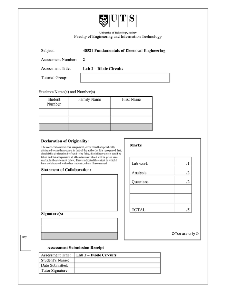
Faculty of Engineering and Information Technology Subject: 48521 Fundamentals of Electrical Engineering Assessment Number: 2 Assessment Title: Lab 2 – Diode Circuits Tutorial Group: Students Name(s) and Number(s) Student Number Family Name First Name Declaration of Originality: The work contained in this assignment, other than that specifically attributed to another source, is that of the author(s). It is recognised that, should this declaration be found to be false, disciplinary action could be taken and the assignments of all students involved will be given zero marks. In the statement below, I have indicated the extent to which I have collaborated with other students, whom I have named. Statement of Collaboration: Marks Lab work /1 Analysis /2 Questions /2 TOTAL /5 Signature(s) Office use only key Assessment Submission Receipt Assessment Title: Student’s Name: Date Submitted: Tutor Signature: Lab 2 – Diode Circuits L2.1 Lab 2 – Diode Circuits Diode characteristic. Half-wave rectifier. Clamp circuit. Voltage doubler. Limiting circuit. Introduction The diode is one of the simplest electronic devices available. However, it’s terminal i-v characteristic is non-linear, and we need to sometimes model the diode to determine a circuit’s behaviour. We will measure a diode’s characteristic, then model the diode (obtain equivalent circuits for the forward-bias and reverse-bias cases). Then we will examine some very important diode applications, and relate what we get in practice to what is predicted from our diode model. One of the most important applications of the diode is in rectification. We will examine the operation and performance of a simple half-wave rectifier. Three other useful applications of diodes will then be examined: the clamp, the voltage doubler, and a limiting circuit. We will also measure the terminal characteristics of a Zener diode, and examine its operation as a voltage regulator. Objectives 1. To measure a signal diode’s and a Zener diode’s i-v characteristic, and to derive linear models for each (in both the forward and reverse biased cases). 2. To observe the behaviour of some simple diode circuits, and to compare experimental behaviour of the circuit with that predicted by the model. Fundamentals of Electrical Engineering Spring 2010 L2.2 Equipment 1 Digital Storage Oscilloscope (DSO) – Hewlett Packard HP54621A 1 function generator (FG) – GFG-8016G or GFG-8020G or GFG-8016D 1 curve tracer adapter (CTA) –Goodwill GCTA-1212A 1 digital multimeter – GW GDM-8045G or GW GDM-8135 2 x 1N914 signal diodes 1 x 4V7 Zener diode 1 x 1 k resistor 1 x 10 k resistor 2 x 1 F capacitors 1 Breadboard Hook-up wire 2 x 4mm to BNC leads Safety Cat. A lab This is a Category A laboratory experiment. Please adhere to the Category A safety guidelines (issued separately). Fundamentals of Electrical Engineering Spring 2010 L2.3 Lab Work [1 mark] Diode Characteristics To examine a diode’s characteristic, we will use a curve tracer. This will give us both the forward-bias and reverse-bias characteristic from which we can derive linear models. In the Lab – Setting up the Curve Tracer 1. Set the following on the curve tracer: Setting up the CTA POWER OFF POLARITY DIODE FORWARD CURRENT LIMIT SIGNAL H-LENGTH fully clockwise BASE CURRENT 10 A COLLECTOR SWEEP VOLTAGE 10 V TRANS / FET TRANS SELECTOR A 2. On the left-hand side, the 1N914 signal diode should be connected to the terminals labelled C and E. The signal diode package has a coloured band (usually black) at the cathode end. The signal diode is smaller than the Zener diode. Fundamentals of Electrical Engineering Spring 2010 L2.4 In the Lab – Setting up the DSO 1. Turn the DSO on. 2. In the File section, press the Save-Recall button, then choose the softkey Default Setup. This will ensure the DSO is a known state, e.g. all probe ratios are restored to 1:1, trigger set to Ch 1, etc. 3. Connect Channel 1 of the DSO to the HORIZONTAL output of the CTA. Connect Channel 2 of the DSO to the VERTICAL output of the CTA. Setting up the DSO 4. Set the DSO to X-Y mode (Push the Main-Delayed button, then choose the softkey XY). This now means that the two signals applied to Channel 1 and 2 will provide the X deflection and Y deflection. (Normally the X deflection is an internally generated signal that sweeps across in a certain amount of time). 5. Push the Acquire key (in the Waveform section) and choose Averaging to reduce the noise on the display. Fundamentals of Electrical Engineering Spring 2010 L2.5 In the Lab – Signal Diode Characteristic 1. Turn the CTA on. 2. For Channel 1: Set the Volts / div to 0.2 V / div, and use the Vertical Position knob to set a 1 V offset. 3. For Channel 2: Set the Volts / div to 0.2 V / div, and use the Vertical Position knob to set a 0.6 V offset. 4. You should see the characteristic of the signal diode, which is similar to that shown below. If your characteristic appears to be going “down” instead of “up”, you will have to invert Channel 2 to obtain a correct polarity for the vertical scale (some CTAs have output inverters, some don’t). To invert Channel 2, push the channel 2 button, then select the softkey Invert. i D ~ vD Characteristic 200 180 160 iD (mA) 140 120 100 80 60 40 20 0 0.1 0.2 0.3 0.4 0.5 0.6 vD (V) Fundamentals of Electrical Engineering Spring 2010 0.7 L2.6 5. Accurately sketch the diode’s forward iD ~ vD characteristic, noting both horizontal and vertical scales. Signal diode forward characteristic Remember: the vertical scale on the DSO is the voltage across the internal 100 resistor of the CTA, so you will have to scale the vertical voltage to get the current. 6. Set the POLARITY BACKWARD. switch of the CTA to PNP / P-CHANNEL / DIODE This will give us the reverse-bias characteristic of the diode. 7. Set the Channel 1 attenuation to 2 V/div, and move the trace to the right of the display using the Channel 1 position knob. 8. Accurately sketch the diode’s reverse iD ~ vD characteristic, noting both horizontal and vertical scales. Signal diode reverse characteristic 9. Move the POLARITY switch on the CTA several times to observe both the reverse and forward characteristics. Fundamentals of Electrical Engineering Spring 2010 L2.7 Questions – Signal Diode Equivalent Circuit 1. Approximate the forward characteristic curve you have drawn with two straight lines. Derive an equivalent circuit model of the diode using a voltage source and a resistance in series. Show all component values. Signal diode forwardbias equivalent circuit Answer: 2. Approximate the reverse characteristic curve you have drawn with one straight line. Derive an equivalent circuit model of the diode using a linear circuit element. Show all component values. Signal diode reversebias equivalent circuit Answer: Fundamentals of Electrical Engineering Spring 2010 L2.8 In the Lab – Zener Diode Characteristic 1. Replace the 1N914 signal diode with the 4.7V Zener diode. Set the polarity switch of the CTA to “NPN / n-channel / diode forward”. This will give us the forward-bias characteristic of the diode. 2. Set the Channel 1 attenuation knob to 0.2 V/div. 3. Accurately sketch the diode’s forward i-v characteristic, noting both horizontal and vertical scales. Zener diode forward characteristic Remember: the vertical scale on the DSO is the voltage across the internal 100 resistor of the CTA, so you will have to scale the vertical voltage to get the current. 4. Set the polarity switch of the CTA to “PNP / p-channel / diode backward”. This will give us the reverse-bias characteristic of the diode. 5. Set the Channel 1 attenuation knob to 1 V/div. Fundamentals of Electrical Engineering Spring 2010 L2.9 6. Accurately sketch the diode’s reverse i-v characteristic, noting both horizontal and vertical scales. Zener diode reverse characteristic 7. Move the “Polarity” switch on the CTA several times to observe both the reverse and forward characteristics. 8. Disconnect the CTA from the DSO. 9. Turn the CTA off and remove the diode. Fundamentals of Electrical Engineering Spring 2010 L2.10 Questions – Zener Diode Equivalent Circuit 1. Approximate the forward characteristic curve you have drawn with two straight lines. Derive an equivalent circuit model of the Zener diode when it is forward-biased. Show all component values. Zener diode forwardbias equivalent circuit Answer: 2. Approximate the reverse characteristic curve you have drawn with two straight lines. Derive an equivalent circuit model of the Zener diode when it is reverse-biased. Show all component values. Zener diode reversebias equivalent circuit Answer: Fundamentals of Electrical Engineering Spring 2010 L2.11 Half-Wave Rectifier (HWR) Rectification of an AC voltage is used to make a DC power supply. An AM radio receiver uses a diode to “peak detect” the incoming radio signals. In both of these cases, a half-wave rectifier is an integral part of the circuit. In the Lab – HWR 1. Set the DSO back to normal operation (not X-Y mode) and set the time base to 0.5 ms/div. 2. If you previously inverted channel 2 to measure the diode characteristics, then turn Invert for channel 2 off. 3. Set the two channels’ attenuations to 2 V/div. 4. Turn the function generator (FG) on. 5. Connect the FG’s output to Channel 1 of the DSO. Set up a 500 Hz sinusoidal waveform with a 5 V amplitude. Ensure there is no DC component in the FG’s output. (Adjust with DC offset knob if necessary). 6. Wire the following circuit on the breadboard. HWR circuit 1N914 1 k 5cos(1000 t ) vi Ch. 1 10 k Fundamentals of Electrical Engineering Spring 2010 vo Ch. 2 L2.12 7. Sketch the vi and vo waveforms below. HWR waveforms 8. Use the cursors of the DSO to measure the “cut-in” angle: Fundamentals of Electrical Engineering Spring 2010 L2.13 Questions – HWR 1. Explain how the circuit works. Operation of HWR circuit Answer: 2. Explain the “cut-in” angle, and compare the experimental value with the theoretical value. Cut-in angle Answer: Fundamentals of Electrical Engineering Spring 2010 L2.14 In the Lab – Filtered HWR (peak detector) 1. Add a capacitor in parallel with the load resistance as shown below. Filtered HWR circuit 1N914 1 k 5cos(1000 t ) vi Ch. 1 10 k vo Ch. 2 2. Sketch the vi and vo waveforms. Filtered HWR waveforms Fundamentals of Electrical Engineering Spring 2010 1 F L2.15 3. Set the DSO channel 2 coupling to AC (AC Coupling). Set the DSO channel 2 attenuation to 0.2 V/div. Sketch the resulting ripple waveform. Ripple voltage 4. Measure the voltage from peak-to-peak: Vr Fundamentals of Electrical Engineering Spring 2010 L2.16 Questions – Filtered HWR (peak detector) 1. Explain how the circuit works. Explain the unusual shape of the vi waveform. Compare Vr with the theoretical value. Operation of filtered HWR circuit Answer: Fundamentals of Electrical Engineering Spring 2010 L2.17 Clamp Circuit A clamp circuit is useful to prevent a waveform from either going negative or positive, or to restore a DC component of a waveform. In the Lab – Clamp Circuit 1. Ensure the DSO’s input couplings are set to DC (Direct Coupling). 2. Set the DSO’s vertical attenuations to 5 V/div. 3. Wire the following circuit on the breadboard. Clamp circuit 1 k 5cos(1000 t ) vi Ch. 1 1 F 1N914 vo Ch. 2 4. Sketch the vi and vo waveforms. Clamp circuit waveforms Fundamentals of Electrical Engineering Spring 2010 L2.18 Questions – Clamp Circuit 1. Explain how the circuit works. Operation of clamp circuit Answer: Fundamentals of Electrical Engineering Spring 2010 L2.19 Voltage Doubler A voltage doubler is a convenient way to obtain a voltage higher than that normally available from a HWR. It is essentially a clamp circuit followed by a peak detector. In the Lab – Voltage Doubler 1. Wire the following circuit on the breadboard. Voltage doubler circuit 1 k vi Ch. 1 1 F 1N914 1N914 10 k 1 F vo Ch. 2 2. Sketch the vi and vo waveforms. Voltage doubler waveforms Fundamentals of Electrical Engineering Spring 2010 L2.20 Questions – Voltage Doubler 1. Explain how the circuit works. Operation of voltage doubler Answer: Fundamentals of Electrical Engineering Spring 2010 L2.21 Limiting Circuit A limiting circuit is useful to prevent a waveform from either going above or below a certain value. One use is in protecting other circuits which may be damaged by an excessive voltage, such as an A/D converter. In the Lab – Limiting Circuit 1. Set the DSO’s vertical attenuations to 5 V/div. 2. Wire the following circuit on the breadboard. Note that channel 1 of the DSO has moved, and that the source voltage has increased. Limiting circuit 1 k 10cos(1000 t) vi Ch. 1 4V7 Zener vo Ch. 2 3. Sketch the vi and vo waveforms. Limiting circuit waveforms Fundamentals of Electrical Engineering Spring 2010 L2.22 Questions – Limiting Circuit 1. Explain how the circuit works. Operation of limiting circuit Answer: In the Lab – Packing Up You don’t complete the lab until you pack up 1. Please pack up all the equipment, and leave the bench tidy. 2. See a lab tutor to ensure your attendance at this lab is recorded. Fundamentals of Electrical Engineering Spring 2010 L2.23 Questions [2 marks] Encircle the correct answer, cross out the wrong answers. [one or none correct] All questions are worth 0.2 marks each. (i) a p n b The diode is: (a) Forward biased and a b a b (b) Forward biased and (c) Reverse biased and a b (ii) 1N914 The output vo is vs vi vo equal to: (b) vi ed (a) vi (c) 0 (iii) The PIV of each diode of a "bridge" full-wave rectifier ( vi = transformer secondary volts) is: (a) vi (c) vˆi 2 (b) 2v̂i (iv) The diffusion capacitance of a forward biased diode (I = diode current): (a) increases with I (b) is independent of I (c) decreases as I increases (v) 2R s vo vs The output vo has Rs 10 R s 2v s (a) 25 16 v̂s (b) 0 peak: (c) 20 11 Fundamentals of Electrical Engineering Spring 2010 v̂s L2.24 (vi) vi R vo The transfer 1N914 characteristic is: E vo vo vo E E +0.7 vi vi slope = 1 vi -0.7 -0.7 (c) (b) (a) (vii) ideal The output vo is vi vo ideal (b) v̂i (a) vi equal to: (c) 2v̂i (viii) 1 2 3 4 In the positive half vi cycle of vi , the “on” diodes are: (a) 1, 3 (b) 2, 4 (c) 2, 3 (ix) vi 6V -4 V vi vo C t In the steady-state, the maximum output, vo max , is: (a) 6 V (b) 4 V (c) 0 V (x) The ripple voltage of a loaded HWR with a filter capacitor is: (a) vˆo 2 fRC (b) vˆo fRC (c) 0 Fundamentals of Electrical Engineering Spring 2010 L2.25 Report Only submit ONE report per lab group. Complete the assessment cover sheet. Ensure you have completed: 1. Lab Work – waveforms, meter readings, calculations. 2. Analysis – explanations where required. 3. Questions – multiple choice questions. The lab report is due at the time stated in the Learning Guide. You should hand the report directly to your tutor. Fundamentals of Electrical Engineering Spring 2010
