Analog Datasheet
802.11n/ac/ad Tri-Band Analog Front End (AFE) IP
TSMC 28HPM
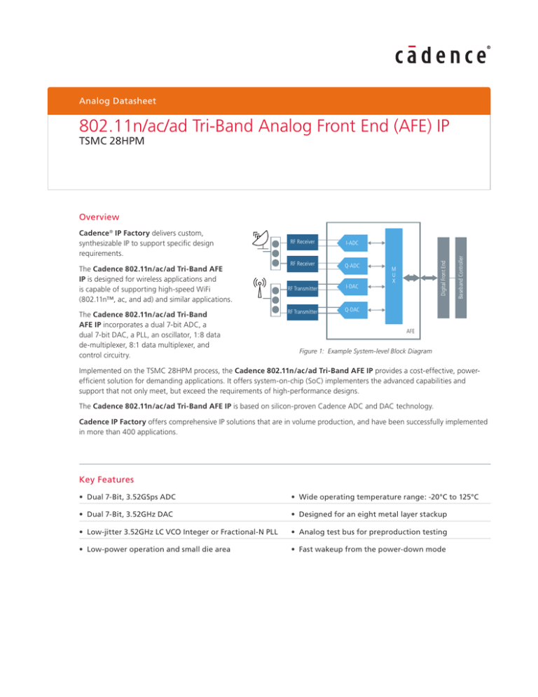
The Cadence 802.11n/ac/ad Tri-Band AFE
IP is designed for wireless applications and
is capable of supporting high-speed WiFi
(802.11n™, ac, and ad) and similar applications.
The Cadence 802.11n/ac/ad Tri-Band
AFE IP incorporates a dual 7-bit ADC, a
dual 7-bit DAC, a PLL, an oscillator, 1:8 data
de-multiplexer, 8:1 data multiplexer, and
control circuitry.
RF Receiver
I-ADC
RF Receiver
Q-ADC
RF Transmitter
I-DAC
RF Transmitter
Q-DAC
M
U
X
Baseband Controller
Cadence® IP Factory delivers custom,
synthesizable IP to support specific design
requirements.
Digital Front End
Overview
AFE
Figure 1: Example System-level Block Diagram
Implemented on the TSMC 28HPM process, the Cadence 802.11n/ac/ad Tri-Band AFE IP provides a cost-effective, powerefficient solution for demanding applications. It offers system-on-chip (SoC) implementers the advanced capabilities and
support that not only meet, but exceed the requirements of high-performance designs.
The Cadence 802.11n/ac/ad Tri-Band AFE IP is based on silicon-proven Cadence ADC and DAC technology.
Cadence IP Factory offers comprehensive IP solutions that are in volume production, and have been successfully implemented
in more than 400 applications.
Key Features
• Dual 7-Bit, 3.52GSps ADC
• Wide operating temperature range: -20°C to 125°C
• Dual 7-Bit, 3.52GHz DAC
• Designed for an eight metal layer stackup
• Low-jitter 3.52GHz LC VCO Integer or Fractional-N PLL
• Analog test bus for preproduction testing
• Low-power operation and small die area
• Fast wakeup from the power-down mode
Product Details
The Cadence 802.11n/ac/ad Tri-Band AFE IP is characterized by
low-power operation and small die area, which makes it suitable
for wireless WiGig® applications.
adc_datai
ADC and DAC Blocks
adc_dataq
The Cadence 802.11n/ac/ad Tri-Band AFE IP incorporates a
dual 7- bit ADC and a dual 7-bit DAC that can support sample
rates up to 3.52GSps. The dual ADC and dual DAC are both
internally synchronized for optimum performance for use in I and
Q modulation communication systems.
Crystal Oscillator Circuit
64
64
7-bit
Q ADC
7
ADC
Interface
7
7-bit
I ADC
adc_vcm
adc_inq_p
adc_inq_m
adc_ini_p
adc_ini_m
OSC
iqadc_clk
pll_clk5
dac_datai
iqdac_clk
PLL
pll_clk6
dac_dataq
The Cadence 802.11n/ac/ad Tri-Band AFE IP contains a
low-jitter 54MHz output crystal oscillator circuit, which can
operate in either a fundamental or a 3rd overtone configuration.
Common
ADC
Control
adc_control
7
56
56
7-bit
Q DAC
DAC
Interface
7
7-bit
I DAC
DAC
Control
dac_control
dac_outq_p
dac_outq_m
dac_outi_p
dac_outi_m
Common
PLL Block
The Cadence 802.11n/ac/ad Tri-Band AFE IP contains a
3.52GHz PLL, which can operate in either an Integer- or a
Fractional-N mode. The PLL utilizes an LC VCO architecture to
enable high-performance, low-jitter AFE operation. With the PLL
and OSC circuit being designed for fast wake up time, the system
can go into sleep mode to save power and wake up to check for
activities.
Figure 2: IP-level Block Diagram
Cadence IP Factory
Cadence IP Factory can deliver various configurations of AFE IP
to meet your design requirements.
With 10+ years of experience and 400+ successful designs in
process nodes ranging from 180nm to 16nm, Cadence IP has been
proven in everything from low-power MP3 players to leading edge
supercomputers.
For more information, visit ip.cadence.com
Available Products
Part Number
Process
Analog Supply Voltage
(V)†
Digital Supply
Voltage(V)
Junction Temperature
(˚C)
RMS Jitter (ps)
IP9936
TSMC 28HPM
0.85 – 0.99, 1.62 – 1.98
0.81 – 0.99
-20 – 125
0.5 (typ.)
† – AVDD, AVDD_H
Benefits
Deliverables
• Fully-integrated solution with clock distribution
• FE views— .lib file, Verilog
• Power-efficient—low power and small die-area
• GDSII, netlist (Cadence Physical Verification System for LVS
and DRC)
• Architecture-efficient—includes ESD Cells and wiring to
bumps
• Low-risk solution— based upon long history of Cadence
high-performance, proven data converter technology
• Footprint (LEF)
• User documentation, integration guidelines, engineering
datasheet
• Silicon validation report (where available)
• Integration support
Cadence Design Systems enables global electronic design innovation and plays an essential role in the
creation of today’s electronics. Customers use Cadence software, hardware, IP, and expertise to design
and verify today’s mobile, cloud, and connectivity applications. www.cadence.com
The IP described in this document may only be taped out and manufactured at a TSMC approved manufacturing facility. Any IC developed from
this IP Core must include layer 63 and any other tagging layers (including all tracking tags) as required by TSMC.
© 2014 Cadence Design Systems, Inc. All rights reserved worldwide. Cadence and the Cadence logo are registered trademarks of Cadence Design
Systems, Inc. in the United States and other countries. All other trademarks are the property of their respective owners.
V2.0 09/14


