Luminescent spin-valve transistor
advertisement

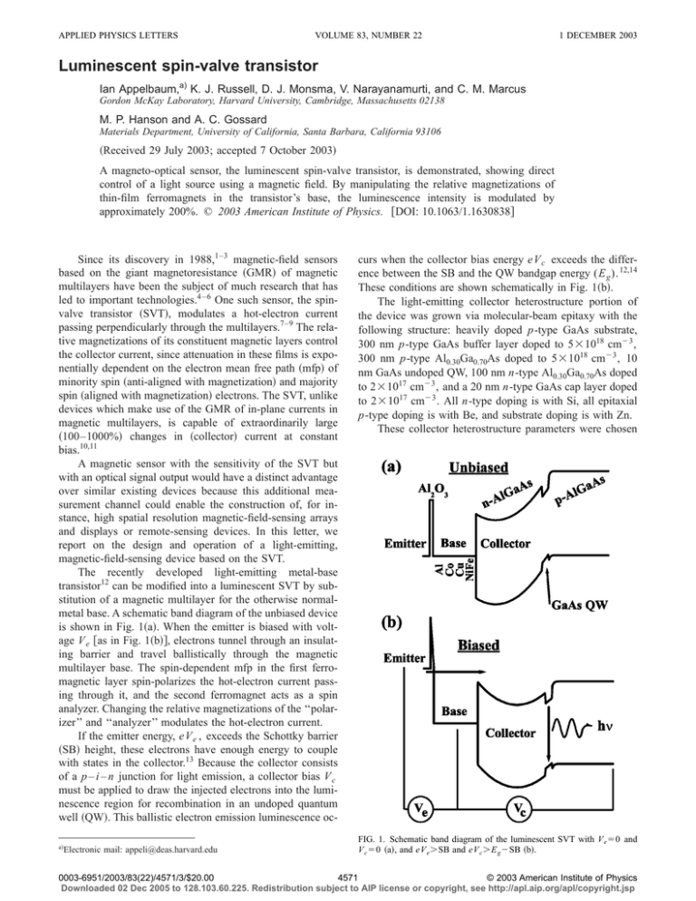
APPLIED PHYSICS LETTERS VOLUME 83, NUMBER 22 1 DECEMBER 2003 Luminescent spin-valve transistor Ian Appelbaum,a) K. J. Russell, D. J. Monsma, V. Narayanamurti, and C. M. Marcus Gordon McKay Laboratory, Harvard University, Cambridge, Massachusetts 02138 M. P. Hanson and A. C. Gossard Materials Department, University of California, Santa Barbara, California 93106 共Received 29 July 2003; accepted 7 October 2003兲 A magneto-optical sensor, the luminescent spin-valve transistor, is demonstrated, showing direct control of a light source using a magnetic field. By manipulating the relative magnetizations of thin-film ferromagnets in the transistor’s base, the luminescence intensity is modulated by approximately 200%. © 2003 American Institute of Physics. 关DOI: 10.1063/1.1630838兴 Since its discovery in 1988,1–3 magnetic-field sensors based on the giant magnetoresistance 共GMR兲 of magnetic multilayers have been the subject of much research that has led to important technologies.4 – 6 One such sensor, the spinvalve transistor 共SVT兲, modulates a hot-electron current passing perpendicularly through the multilayers.7–9 The relative magnetizations of its constituent magnetic layers control the collector current, since attenuation in these films is exponentially dependent on the electron mean free path 共mfp兲 of minority spin 共anti-aligned with magnetization兲 and majority spin 共aligned with magnetization兲 electrons. The SVT, unlike devices which make use of the GMR of in-plane currents in magnetic multilayers, is capable of extraordinarily large 共100–1000%兲 changes in 共collector兲 current at constant bias.10,11 A magnetic sensor with the sensitivity of the SVT but with an optical signal output would have a distinct advantage over similar existing devices because this additional measurement channel could enable the construction of, for instance, high spatial resolution magnetic-field-sensing arrays and displays or remote-sensing devices. In this letter, we report on the design and operation of a light-emitting, magnetic-field-sensing device based on the SVT. The recently developed light-emitting metal-base transistor12 can be modified into a luminescent SVT by substitution of a magnetic multilayer for the otherwise normalmetal base. A schematic band diagram of the unbiased device is shown in Fig. 1共a兲. When the emitter is biased with voltage V e 关as in Fig. 1共b兲兴, electrons tunnel through an insulating barrier and travel ballistically through the magnetic multilayer base. The spin-dependent mfp in the first ferromagnetic layer spin-polarizes the hot-electron current passing through it, and the second ferromagnet acts as a spin analyzer. Changing the relative magnetizations of the ‘‘polarizer’’ and ‘‘analyzer’’ modulates the hot-electron current. If the emitter energy, eV e , exceeds the Schottky barrier 共SB兲 height, these electrons have enough energy to couple with states in the collector.13 Because the collector consists of a p – i – n junction for light emission, a collector bias V c must be applied to draw the injected electrons into the luminescence region for recombination in an undoped quantum well 共QW兲. This ballistic electron emission luminescence oca兲 Electronic mail: appeli@deas.harvard.edu curs when the collector bias energy eV c exceeds the difference between the SB and the QW bandgap energy (E g ). 12,14 These conditions are shown schematically in Fig. 1共b兲. The light-emitting collector heterostructure portion of the device was grown via molecular-beam epitaxy with the following structure: heavily doped p-type GaAs substrate, 300 nm p-type GaAs buffer layer doped to 5⫻1018 cm⫺3 , 300 nm p-type Al0.30Ga0.70As doped to 5⫻1018 cm⫺3 , 10 nm GaAs undoped QW, 100 nm n-type Al0.30Ga0.70As doped to 2⫻1017 cm⫺3 , and a 20 nm n-type GaAs cap layer doped to 2⫻1017 cm⫺3 . All n-type doping is with Si, all epitaxial p-type doping is with Be, and substrate doping is with Zn. These collector heterostructure parameters were chosen FIG. 1. Schematic band diagram of the luminescent SVT with V e ⫽0 and V c ⫽0 共a兲, and eV e ⬎SB and eV c ⬎E g ⫺SB 共b兲. 0003-6951/2003/83(22)/4571/3/$20.00 4571 © 2003 American Institute of Physics Downloaded 02 Dec 2005 to 128.103.60.225. Redistribution subject to AIP license or copyright, see http://apl.aip.org/apl/copyright.jsp 4572 Appl. Phys. Lett., Vol. 83, No. 22, 1 December 2003 FIG. 2. Optical profile of the 900⫻900 m2 luminescent SVT. The two triangular-shaped structures form tunnel junction and ohmic contact to the underlying 500⫻500 m2 magnetic multilayer base. The ‘‘⬎’’-shaped region is an insulating layer for wire bonding. The small diamond shape is an alignment mark. to provide an n-type Schottky interface at the surface and a hole-rich recombination region in the otherwise undoped GaAs QW. The n-type surface doping is required so that the injected electrons have long lifetimes as majority carriers before recombining radiatively in the QW. Additionally, the doping results in a built-in field which pulls electrons into the semiconductor. This doping must be relatively low to ensure Schottky contact, but not so low that the surface depletion region extends into the p – i – n junction, which would cause leakage upon reverse biasing. The p-type doping level beneath the undoped QW must be significantly higher than that of the n-type region to compensate the electron population in the QW. The wafer was processed using standard shadow-mask and photolithographic techniques to fabricate SVTs. After cleaning the surface with dilute NH4 OH, a magnetic multilayer consisting of 50 Å Ni84Fe16 , 50 Å Cu, 50 Å Co, 100 Å Al was then deposited via thermal evaporation at high vacuum to form a 500⫻500 m2 base Schottky contact. Next, 1000 Å of Al2 O3 was deposited via electron-beam evaporation over a portion of the multilayer base to form an insulating region. To grow the tunnel oxide, the sample was exposed for 300 s to UV O3 . Two 600 Å Al emitters were deposited via thermal evaporation, partially on the Al2 O3 insulator for wire bonding. These conductors form two tunnel junctions on the base layer. The sample was then processed into device mesas approximately 2 m high and of area 900⫻900 m2 by patterning with photolithography and etching with NH4 OH/H2 O2 /H2 O 1:1:5 for 45 s. An image of the completed device taken with an interferometric optical profiler is shown in Fig. 2. Electrical contact to the collector substrate was made by cold-pressing In into the back surface. Wire bonds to the two Al stripes provide emitter and base contacts after ramping a current through both tunnel junctions until one shorted. All measurements were done in an optical cryostat at 77 K. The luminescence was collected with a 0.2 numerical aperture lens, and the spectra were recorded with a Thermo-Oriel MS257 spectrograph with a cooled CCD camera, a diffraction grating with 150 lines/mm, and a blaze wavelength of 800 nm. Appelbaum et al. FIG. 3. Spectra of emitted luminescence under constant emitter and collector voltages, with magnetic field such that the magnetizations of the ferromagnetic layers are parallel (⫺200 G) and antiparallel 共30 G兲. The luminescent SVT is operated at constant emitter bias and collector bias. An emitter bias energy far greater than the SB (⬇0.8 eV) is needed to inject a substantial hot-electron current, but this voltage must be kept lower than the breakdown voltage for the tunnel junction; we use V e ⫽⫺1.7 V, which gives an emitter–base current of 2.6 mA. A collector bias energy exceeding the difference between the QW bandgap energy (⬇1.5 eV) and the SB (⬇0.8 eV) is needed to partially null the built-in field at the p – i – n junction; we use V c ⫽0.9 V. At an applied external magnetic field (⫺200 G) in excess of the coercive fields of Ni84Fe16 and Co, the magnetizations of the ferromagnetic layers are aligned parallel. The hot electrons traveling through the base have a long mfp in both ferromagnetic layers, and a relatively large fraction of electrons can couple with semiconductor conduction band states and radiatively recombine in the QW, emitting light. Figure 3 shows the optical spectrum of this luminescence. After reducing the magnetic field to zero and then increasing in the opposite direction to a value 共30 G兲 between the two coercive fields, the magnetizations are aligned antiparallel and inelastic scattering in the base attenuates the hot-electron current, leading to a reduced optical signal, also shown in Fig. 3. Cycling the external field and measuring the collector current yields a hysteresis curve typical of SVTs, as shown in Fig. 4共a兲. A collector current change of ⬇133% is evident from this data. Simultaneous collection of emitted luminescence spectra allows the construction of a similar hysteresis curve shown in Fig. 4共b兲, where the peak heights of the collected luminescence spectra are plotted on the same magnetic field axis as Fig. 4共a兲. The two hysteresis curves have a similar shape, but Fig. 4共b兲 shows a luminescence change of ⬇200%, significantly more than the collector current change shown in Fig. 4共a兲. This suggests that, whereas the luminescence is due only to hot electrons injected into the conduction band, the collector current is at least partially due to an induced leakage current which dilutes the change in collector current. These data show that the light emitted from a luminescent spin-valve transistor can be used as a complimentary signal channel yielding information about the magnetic field. Downloaded 02 Dec 2005 to 128.103.60.225. Redistribution subject to AIP license or copyright, see http://apl.aip.org/apl/copyright.jsp Appelbaum et al. Appl. Phys. Lett., Vol. 83, No. 22, 1 December 2003 4573 optically-read magnetic random access memory, and read heads for magnetic hard drives interfaced with optical networks. The authors acknowledge support from the NSF under #ECS-9906047, the ONR under #N00014-02-1-0994 and the Harvard NSEC and MRSEC. This material is based upon work supported by the Defense Advanced Research Programs Agency 共DARPA兲 under Award No. MDA972-01-10024 and The California Institute of Technology. 1 FIG. 4. Simultaneously collected hysteresis curves for collector current 共a兲 and luminescence spectrum peak 共b兲 at constant emitter and collector bias. If the low luminescence signal can be increased by enhancing the observed luminescence efficiency 共for instance, by changing the QW material or using a Bragg reflector deep within the collector兲 or by increasing the collector current 共for instance, by implementing high-voltage avalanche multiplication in the collector Schottky depletion region兲, we expect this type of device to be useful for remote-sensing magnetic fields, magnetic-field visualization displays, H. Sato, P. A. Schroeder, J. Slaughter, W. P. Pratt, Jr., and W. AbdulRazzaq, Superlattices Microstruct. 4, 45 共1988兲. 2 M. N. Baibich, J. M. Broto, A. Fert, F. Nguyen Van Dau, F. Petroff, P. Eitenne, G. Creuzet, A. Friederich, and J. Chazelas, Phys. Rev. Lett. 61, 2472 共1988兲. 3 G. Binasch, P. Grunberg, F. Saurenbach, and W. Zinn, Phys. Rev. B 39, 4828 共1988兲. 4 S. A. Wolf and D. M. Treger, Proc. IEEE 91, 647 共2003兲. 5 S. S. P Parkin, X. Jiang, C. Kaiser, A. Panchula, K. Roche, and M. Samant, Proc. IEEE 91, 661 共2003兲. 6 E. Hirota, H. Sakakima, and K. Inomata, Giant Magneto-Resistance Devices 共Springer, New York, 2001兲. 7 D. J. Monsma, J. C. Lodder, Th. J. A. Popma, and B. Dieny, Phys. Rev. Lett. 74, 5260 共1995兲. 8 D. J. Monsma, R. Vlutters, and J. C. Lodder, Science 281, 407 共1998兲. 9 K. Mizushima, T. Kinno, T. Yamauchi, and K. Tanak, IEEE Trans. Magn. 33, 3500 共1997兲. 10 O. M. J. van’t Erve, R. Vlutters, P. S. A. Kumar, S. D. Kim, F. M. Postma, R. Jansen, and J. C. Lodder, Appl. Phys. Lett. 80, 3787 共2002兲. 11 S. van Dijken, X. Jiang, and S. S. P. Parkin, Appl. Phys. Lett. 82, 775 共2003兲. 12 I. Appelbaum, K. J. Russell, V. Narayanamurti, D. J. Monsma, C. M. Marcus, M. P. Hanson, A. C. Gossard, H. Temkin, and C. H. Perry, Appl. Phys. Lett. 82, 4498 共2003兲. 13 J. P. Spratt, R. F. Schwarz, and W. M. Kane, Phys. Rev. Lett. 6, 341 共1961兲. 14 K. J. Russell, I. Appelbaum, H. Temkin, C. H. Perry, V. Narayanamurti, M. P. Hanson, and A. C. Gossard, Appl. Phys. Lett. 82, 2960 共2003兲. Downloaded 02 Dec 2005 to 128.103.60.225. Redistribution subject to AIP license or copyright, see http://apl.aip.org/apl/copyright.jsp


