Gigabit Ethernet Multimode Small Form-Factor
Gigabit Ethernet Multimode
Small Form–Factor Pluggable
(SFP) MT–RJ Transceivers
Application Specification
114–13081
11 AUG 03 Rev A
NOTE
All numerical values are in metric units [with U.S. customary units in brackets]. Dimensions are in millimeters [and inches]. Unless otherwise specified, dimensions have a tolerance of +0.13 [.005] and angles have a tolerance of +2
_
.
Figures and illustrations are for identification only and are not drawn to scale.
1. INTRODUCTION
This specification covers recommendations for application of Gigabit Ethernet Multimode SFP MT–RJ
Transceivers. The transceiver is an 850 nm vertical cavity surface emitting laser–based (VCSEL) fiber optic device used primarily in Gigabit Ethernet applications. A type MT–RJ connector is provided as the external connector on the optical interface. Gigabit Ethernet can be transmitted and received by these transceivers over a pair of 62.5 m m or 50 m m core multimode optical fibers. The transceiver operates from a single +3.3 Vdc power supply and contains AC coupled transmitter and receiver sections that have positive emitter coupled logic/low voltage positive emitter coupled logic (PECL/LVPECL) compatible data interfaces. Although these transceivers have been specifically designed and tested to meet certain standards, the transceivers can also be used for Fibre Channel applications.
The transceiver (or module) is for use in the network to cable plant interface. An SFP–compatible cage assembly and connector are mounted onto the printed circuit (pc) board. The cage assembly is also mounted through a bezel. The transceiver fits into the cage assembly and is guided to link with the connector. The transceiver is hot swappable (can be installed or removed with the equipment power on or off).
The transceiver features panel ground springs to provide electrical contact to the cage assembly and an ejection mechanism. The housing and case grounds minimize electromagnetic interference (EMI) susceptibility and radiated emissions.
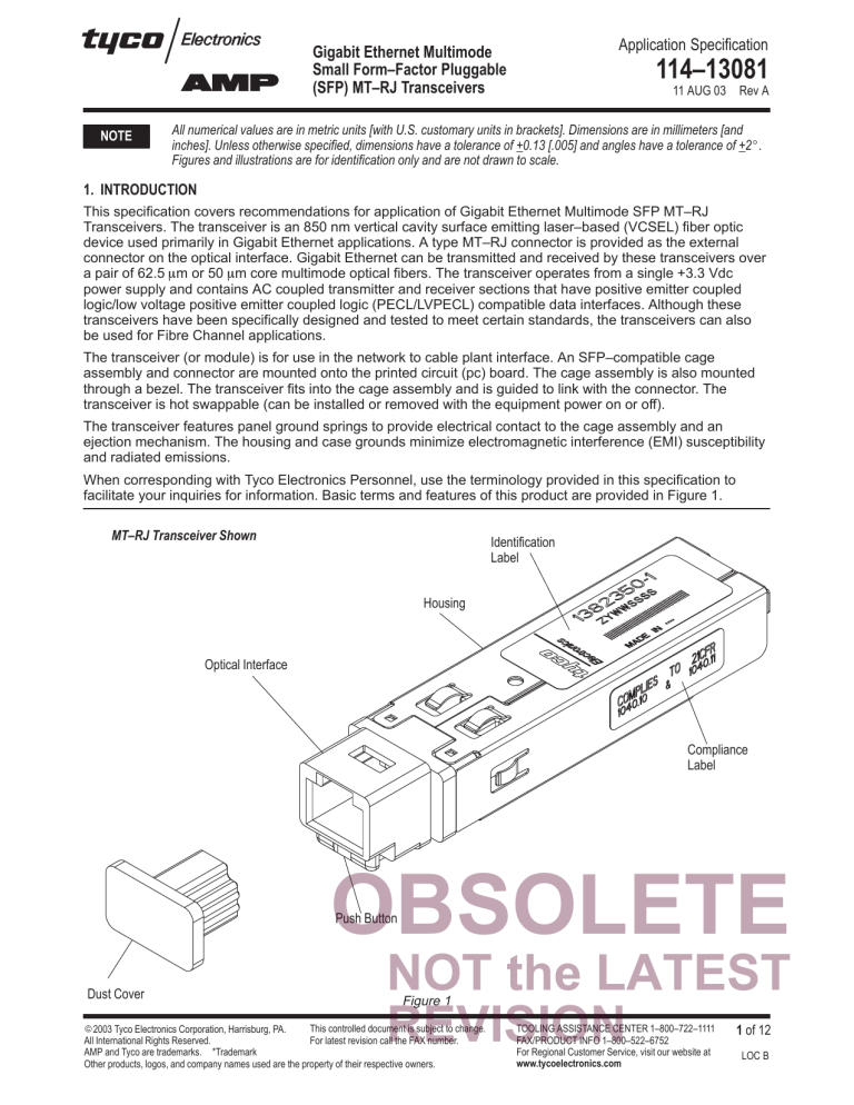
When corresponding with Tyco Electronics Personnel, use the terminology provided in this specification to facilitate your inquiries for information. Basic terms and features of this product are provided in Figure 1.
MT–RJ Transceiver Shown
Identification
Label
Housing
Optical Interface
Compliance
Label
Dust Cover
E
2003 Tyco Electronics Corporation, Harrisburg, PA.
All International Rights Reserved.
AMP and Tyco are trademarks.
*Trademark
NOT the LATEST
Figure 1
REVISION
For latest revision call the FAX number.
Other products, logos, and company names used are the property of their respective owners.
FAX/PRODUCT INFO 1–800–522–6752
For Regional Customer Service, visit our website at www.tycoelectronics.com
1 of 12
LOC B
Gigabit Ethernet Multimode SFP MT–RJ Transceivers 114–13081
2. REFERENCE MATERIAL
2.1. Revision Summary
Per EC 0990–1024–03:
S
Updated document to corporate requirements
S
Changed text in Paragraphs 2.2, 2.3, 3.6, 3.9, and Section 5, TOOLING
S
Changed text in Figures 5 and 6
2.2. Customer Assistance
Reference Product Base Part Number 1382350 and Product Code 6294 are representative of Gigabit Ethernet multimode SFP MT–RJ transceivers. Use of these numbers will identify the product line and expedite your inquiries through a service network established to help you obtain product and tooling information. Such information can be obtained through a Tyco Electronics Representative (Field Service Engineer, Field
Applications Engineer, etc.) or, after purchase, by calling PRODUCT INFO at the number at the bottom of page 1.
2.3. Drawings
Customer Drawings for product part numbers are available from the service network. If there is a conflict between the information contained in the Customer Drawings and this specification or with any other technical documentation supplied, call PRODUCT INFO at the number at the bottom of page 1.
2.4. Specifications
Application Specifications (114–Series) provides product description and application requirements. Documents available which relate to this product are:
114–13017 SFP Connector and Cage Assembly
Product Specification 108–55027 provides product performance and test information.
2.5. Instructional Material
Instruction Sheets (408–series) provide assembly instructions. Documents available which relate to this product are:
408–8429 SFP LC and MT–RJ Transceivers
2.6. Catalogs
Sales Catalogs available are 1308514 (Gigabit Fiber Channel Multimode SFP MT–RJ Transceivers) and
1307895 (Fiber Optic Product Catalog).
2.7. Standards and Publications
Standards and publications developed by the Institute of Electrical and Electronic Engineers, Inc. (IEEE),
American National Standards Institute (ANSI), Telecommunications Industry Association and Electronic
Industries Alliance (TIA/EIA), International Electrotechnical Commission (IEC), and Food and Drug
Administration (FDA) provide industry test and performance requirements. Documents available which pertain to this product are:
IEEE Std. 802.3, Clause 38, “Physical Medium Dependent (PMD) Sublayer and Baseband Medium, Type
1000BASE–Long Wavelength Laser (LX) and 1000BASE–Short Wavelength Laser (SX)”
NOTE
Although these transceivers have been specifically designed and tested to meet this standard, the transceivers can also be used for Fibre Channel applications.
IEEE Std. 802 Annex 36A, “Jitter Test Patterns”
ANSI X3.230, “Information Technology–Fibre Channel–Physical and Signaling Interface (FC–PH)”
TIA/EIA–455–95, “Absolute Optical Power Test for Optical Fibers and Cables”
TIA/EIA–526–4, “Optical Eye Pattern Measurement Procedure”
TIA/EIA–526–14, “Optical Power Loss Measurements of Installed Multimode Fiber Cable Plant —
OFSTP 14A”
2 of 12 Rev A
Gigabit Ethernet Multimode SFP MT–RJ Transceivers 114–13081
TIA/EIA–455–107, “FOTP 107—Determination of Component Reflectance or Link/System Return Loss using a Loss Test Set”
IEC 60825–1, “Part 1: Safety of Laser Products—Equipment Classification, Requirements and User’s
Guide”
IEC 60825–2, “Part 2: Safety of Optical Fiber Communication Systems”
FDA 21 Code of Federal Regulations (CFR) Chapter 1, Part 1040, “Performance Standards for Light
Emitting Products”
NOTE
All products that contain a laser must comply with government regulations for laser safety. In the U.S., the applicable standard is FDA 21 CFR Chapter 1, Part 1040, and outside the U.S., IEC 60825–1 applies. These transceivers are designed and tested to meet the requirements of these standards and found to be in compliance with Class 1 laser safety limits. When operated within the limits specified in this document, this product conforms to IEC 60825–1: 1993
+A1: 1997 +A2: 2001, Class 1 laser product requirements.
2.8. Application Notes
ON SEMICONDUCTOR
TM
AN1406/D, Sept., 1999: Rev 2, “Designing with PECL (ECL at +5.0 V)—The
High Speed Solution for the CMOS/TTL Designer.” Cleon Petty and Todd Person at Semiconductor
Components Industries, LLC (http://www.onsemi.com/pub/Collateral/AN1406–D.PDF)
ON SEMICONDUCTOR TM AN1672/D, May, 2001: Rev 3, “The ECL Translator Guide—ECL, TTL, PECL,
LVECL, LVPECL, CMOS, LVTTL, How to Make Them Talk to Each Other.” Paul Stockman and Paul Hunt at
Semiconductor Components Industries, LLC (http://www.onsemi.com/pub/Collateral/AN1672–D.PDF)
2.9. Miscellaneous
Motorola DL140/D, “High Performance ECL Data Book, ECLinPs and ECLinPs Lite,” provides a comprehensive description of transmission line design and termination techniques.
SFP Multi–Source Agreement (MSA)—The package for the transceiver has been designed to fully comply with the SFP MSA (http://www.schelto.com/SFP/index.html)
3. REQUIREMENTS
DANGER
Use of controls on this product, adjustments made to this product, or performing procedures other than those specified in this document, may result in exposure to hazardous radiation.
3.1. Laser Safety
These transceivers are designed and tested to be in compliance with Class 1 laser safety standards both in the
U.S. and internationally when used within the limits specified in this document for temperature and power supply. These products are inherently safe since prolonged exposure to radiation from such lasers will not cause damage to the skin or eyes.
Laser safety is maintained during normal operation through factory–set adjustments which compensate for the known light of the laser versus current behavior as a function of temperature and power supply voltage. During single point failure conditions, laser safety is preserved by the internal optical subassembly which limits the emitted optical signal and ensures that even at the maximum light output of the VCSEL, the accessible emission will not exceed Class 1 limits.
3.2. Storage
A. Ultraviolet Light
Prolonged exposure to ultraviolet light may deteriorate the chemical composition used in the transceiver material.
B. Shelf Life
The transceivers should remain in the shipping containers until ready for use to prevent deformation. The transceivers should be used on a first in, first out basis to avoid storage contamination that could adversely affect performance.
CAUTION
Do not stack product shipping containers too high that the containers will buckle or deform.
C. Chemical Exposure
Do not store transceivers near any chemical listed below as they may cause stress corrosion cracking.
Rev A 3 of 12
Gigabit Ethernet Multimode SFP MT–RJ Transceivers 114–13081
Alkalies
Amines
Ammonia
Carbonates
Citrates
Nitrites
Phosphates Citrates
Sulfur Nitrites
Sulfur Compounds
Tartrates
3.3. Assembly Precautions
Personnel handling these transceivers or printed circuit (pc) boards containing these transceivers must observe the following precautions during assembly and testing procedures:
S
Electrostatic discharge (ESD) precautions, similar to those used in any modern electronic card, are recommended.
Minimum recommended precautions include the use of a grounded wrist strap and a grounded conductive mat covering the work area.
S
Multiple mating test fixtures should be designed such that the connector ferrules have sufficient alignment float when inserted into the transceivers. An overly rigid, blind mating test fixture may damage the transceivers, test fixture, or both when mating.
S
Ferrules used in testers should be inspected, cleaned, and maintained regularly. Inspection should be performed under sufficient magnification to detect micro–cracks in the fiber. Dry, oil free, filtered compressed air or dry nitrogen is recommended for removing dust and debris from ferrules and interface of the transceivers before connection.
S
The dust cover is designed to prevent dirt and debris from entering the optical interface during assembly; therefore, the dust cover should be inserted into the optical interface during all phases of assembly and should only be removed when a fiber optic cable or test fixture is mated to the transceiver.
3.4. Function
Like the 10 Mb/s ethernet and 100 Mb/s Fast Ethernet, Gigabit Ethernet functionality is grouped according to several distinct layers. The upper layers define the protocol and software operations necessary to allow Gigabit
Ethernet local area networking hardware, such as switches and repeaters, to communicate with one another.
The lower layers define the hardware operations and interface signals which allow the circuitry to function together seamlessly at the circuit board level.
The lowest layer is the physical layer (PHY). The PHY defines the interface between the data transmission device and the physical medium (optical fiber or copper wire) used to carry data from source to destination.
The PHY is further divided into sublayers which include the physical coding sublayer (PC) (8b/10b encoding), the physical medium attachment sublayer (PMA) (serializer/deserializer and clock recovery), and the physical medium dependent sublayer (PMD) (850 nm optics, 1300 nm optics, or copper cable). This transceiver forms the heart of a 1000BASE–SX PHY. See Figure 2.
Gigabit Ethernet PHY
Network
Data Link
Physical
LX MDI
LX–PMD
Medium
GMII
SX MDI
PC
PMA
SX–PMD
Medium
1000BASE–X
PHY
CX MDI
CS–PMD
Medium
1000BASE–LX
(PCs, PMA, LX–PMD)
1000BASE–SX
(PCs, PMA, SX–PMD)
1000BASE–CX
(PCs, PMA, CX–PMD)
Figure 2
PHY sublayer partitioning at the circuit board level is left to the individual preference of the integrated circuit designers. In a real world system, the integrated circuit chips, fiber optic transceiver, cable plant, and connectors are combined to form a complete data communication link. A common approach to fiber optic transceiver–based PHY design is shown in Figure 3.
4 of 12 Rev A
Host
Data Bus
Gigabit Ethernet Multimode SFP MT–RJ Transceivers
Typical Gigabit Ethernet Fiber Optic Transceiver–Based PHY
MAC
Circuitry
Data
Clock
Clock
Data
8B/10B
Encoder
8B/10B
Decoder
Serializer
Clock
Recovery
Deserializer
Tx
Fiber Optic
Transceiver
Rx
114–13081
Figure 3
The transceiver consists of a transmitter and receiver for performing the electro–optic conversions between electrical PECL/LVPECL logic level signals and optical signals. The transmitter consists of an
850 nm VCSEL and a laser driver integrated circuit. The receiver contains a preamplifier with a GaAs PIN photodiode followed by a limiting amplifier with PECL/LVPECL compatible logic outputs. See Figure 4.
VCSELs provide several advantages over edge emitting lasers when used for high speed data transmission.
VCSELs require low drive current for high optical power output which results in decreased heat dissipation in the transmitter circuit. VCSELs also exhibit well behaved circular beam characteristics which leads to simplified alignment between the laser and the optical fiber. Since VCSELs emit light from their surface, as opposed to their edge, they can be easily tested and screened at the wafer level. The same cannot be said for edge emitting devices which must be cleaved into individual die and placed on a submount before testing can be accomplished. A properly designed and manufactured VCSEL is inherently reliable and does not require the rigorous screening associated with high reliability lasers selected for use in data communication systems.
20
V
EEt
Transceiver Functional Block Diagram
T
FAULT
T
DIS
V
CCt
2 3 16
TD+ 18
TD– 19
LVPECL
Input
Buffer
Modulation
Control
Bias
Control
Bias Adjust Network
15
V
CCr
Preamplifier
Limiting
Amplifier
Signal Detect
LVPECL
Output
Buffer
14
V
EEr
Figure 4
13
12
8
RD+
RD–
LOS
Rev A 5 of 12
Gigabit Ethernet Multimode SFP MT–RJ Transceivers 114–13081
The laser driver circuit accepts a digital logic level (PECL/LVPECL) input and provides the proper bias and modulation currents for maintaining the VCSEL within its specified operating range. The receiver accepts an input from the fiber optic cable in the form of a modulated optical signal and converts it to a digital logic
(PECL/LVPECL) output. This signal is focused onto a small area GaAs PIN photodiode which converts the incident light into a proportional photocurrent. The transimpedance preamplifier converts the photocurrent into an analog voltage which is fed to the limiting amplifier (also referred to as a quantizer). The limiting amplifier converts the analog voltage into a digital logic signal that interfaces with external circuitry, such as a PHY chip.
3.5. Loss of Signal (Signal Detect) and Reference Generator
The loss of signal (LOS) circuit compares the signal from the quantizer with a reference generator to determine the presence of an optical signal. The signal is used as a rough link integrity monitor, not a bit error rate (BER) monitor. It is useful for recognizing when the input to the receiver has dropped well below recommended levels.
The comparison is done with hysteresis so that the LOS assert and deassert occur at different power levels.
The difference between the assert and deassert levels provided by the hysteresis ensures chatter–free operation by preventing the signal from toggling between HIGH and LOW if the power levels hover around a certain point. The LOS signal is an open collector output and should be pulled up with an external 4.7K ohm through 10K ohm resistor.
3.6. Transmitter Disable
The transceiver provides an input that turns off the transmitter’s output independent of the data inputs. The transmitter is constantly biased just above its laser threshold level and so unmodulated light is sent across the fiber link when no data is being transmitted. To prevent the possibility of a receiver inadvertently sensing a signal during a period when no data is transmitted, the transmitter can be disabled by connecting this transmitter disable input directly to an external controller. The transmitter disable input is internally pulled up with a 10K ohm resistor; therefore, if the system designer does not prefer to use the transmitter disable function, the pin must be grounded to enable the transmitter.
3.7. Transmitter Fault
This is an open collector output which should be pulled up with an external 4.7K ohm through 10K ohm resistor on the host board. When at logic HIGH, this output indicates a laser fault. When at logic LOW, it indicates normal operation.
3.8. Rate Select
This function is not implemented and the associated pin is floating. This is an optional input and can remain disconnected.
3.9. Data Encoding and AC Coupling
Gigabit Ethernet PHY chips use an encoding scheme known as 8b/10b which is an advantageous way of transmitting data using fiber optic transceivers. This encoding limits the run length (the number of consecutive
1s or 0s) and maintains DC balance by ensuring that, over time, an equal number of 1s and 0s are sent through the link. This is refered to as disparity neutral or balanced data.
The receiver of the transceiver is internally AC coupled. Specifically, there are internal AC coupling capacitors in the data path between the preamplifier and post amplifier which control the lower 3 dB cutoff frequency of the receiver. This is done to limit the low frequency noise response of the receiver and improve sensitivity.
A direct result of AC coupling the receiver is that links, which use these transceivers, will not pass signals at
DC or low frequencies. Long continuous strings of logic 1s or 0s, which have significant low frequency content, will be distorted by an AC coupled link. For this reason, the transceiver requires data to be encoded in a manner which limits the run length such as 8b/10b, asyschronous transfer mode/synchronous optical network
(ATM/SONET) scrambling, etc. This is not a unique characteristic of these transceivers and is common for most commercially available Gigabit fiber optic transceivers.
The transceiver is provided with differential data inputs and outputs and these are both internally AC coupled.
The transmitter input is internally terminated with a 100 ohm differential termination resistor and the receiver output requires that a 100 ohm differential termination resistor be provided on the host board. This provides a
50 ohm single–ended termination impedance and reduces the number of external components required on the application board. See Figure 5.
6 of 12 Rev A
Gigabit Ethernet Multimode SFP MT–RJ Transceivers 114–13081
NOTE
To improve electromagnetic interference (EMI), signals to the connector must be disconnected when the transceiver is removed.
In most applications using optical transceivers, additional high speed circuitry, such as clock oscillators, can be present on the application board. These high speed signals often lead to noise on power supply circuits at a high spectral bandwidth which can affect the performance of transceivers. Even though the transceivers provide electro–magnetic immunity regarding emission, ingress of radiation and immunity against conductive noise must be considered.
When designing the electrical interface between the transceiver and the PHY chip, it is important to terminate the transmission line with the appropriate characteristic impedance (typically 50 ohms). It is also important to pay particular attention to pc board layout practices. Microstrip lines are recommended for optimum transmission signal quality. Termination recommendations are given for 50 ohm transmission lines. The recommended pc board layer structure is shown in Figure 6.
Vcc and GND connections should be made as short as possible. GND islands should be tied to main GND by vias or avoided if possible. Differential signal lines should be as short as possible and of equal length to maintain signal integrity. Transmitter data input lines and receiver data output lines should be kept far apart to prevent crosstalk. These lines can be run orthogonally or separated with a ground plane layer. One way to maintain the separation is to place all components for the transmit circuit on one side of the board and all components for the receive circuit on the other side of the board. Vias and layer changes should be avoided.
The separation between differential traces of each input or output stage can be minimized by using microstrip design rules.
Rev A 7 of 12
Gigabit Ethernet Multimode SFP MT–RJ Transceivers
Power Supply Filtering of the Transceiver
114–13081
3.3 V Protocol Vcc
3.3 V
C1 C2
Protocol Vcc
Tx_Disable
Tx_Fault
LOS
Rup
TX+
TX–
RX+
RX–
See Note
100
Ω
Rup
PLD/PAL Vcc
3.3 V PLD/PLA Vcc
Rup
Rup
Rup
PLD/PAL
L1
L2
VccT
C3
Tx_Disable
Rup
3
Tx_Fault 2
SFP Module
16
C4
TD+ 18
TD– 19
100
Ω
VeeT 1,17,20
VccR 15
C5
RD+ 13
RD– 12
Laser
Driver
Preamp and
Quantizer
LOS 8
Rate Select 7
VeeR 9, 10, 11, 14
Mod_def 0
6
Mod_def 1
5
Mod_def 2
4
Note: Use SERDES IC manufacturer’s termination recommendation.
C1 = C4 = 10 m F
C2 = C3 = C5 = 0.1 m F (X7R or better MLC–type capacitors are recommended)
L1 = L2 = 1 m H .... 4.7 m H max, 1.0 ohm (ferrite inductors may be used)
Rup = 4.7K ohms .... 10K ohms
Figure 5
8 of 12 Rev A
Gigabit Ethernet Multimode SFP MT–RJ Transceivers 114–13081
Recommended PC Board Layer Structure
Signal
Signal Ground (GND)
V
CC
Rx and Tx (Split Plane)
Additional Signal Layers
Ground (GND)
Figure 6
3.10. Transceiver Filtering
Power supplies in the system must be adequately filtered to prevent supply noise from degrading transceiver performance. The theory behind commonly used power supply filtering techniques described in text books and integrated circuit data books is covered in this document.
The recommended filter scheme separates the power supply for the transmitter and receiver. Power supply noise amplitude and frequency content is largely influenced by the type of supply used, high frequency logic and switching circuitry in the system, circuit board design, etc. For this reason, supply filter circuits should be evaluated under actual conditions before finalizing the design. Capacitors should be chosen with low effective series resistance, low dissipation factor and high Q. NPO or COG temperature characteristics are preferred because they provide more reliable performance over a wide range of environmental conditions. X7R types will also give acceptable performance; however, Y5V and Z5U should be avoided due to their large temperature and voltage coefficients. Ferrite beads used for L1 and L2 will provide higher noise attenuation because they do not possess the interwinding capacitance of a wound inductor. Refer to Figure 5.
Small surface–mount packages are recommended since they exhibit less parasitic inductance which can lower the overall effectiveness of the bypass capacitor at high frequencies. Filter capacitors should be placed close to the transceiver power and ground pins to minimize noise coupling which can occur between the filter and the transceiver.
The impedance of power supply and ground lines on the pc board must be kept low. This is necessary because the dynamic current requirements of high speed digital circuitry can interact with a non–zero impedance to cause fluctuations in the voltage delivered to the transceiver. Therefore, this impedance leads to noise on the supply lines in addition to the inherent power supply switching noise. In order to keep the impedance low, the use of dedicated power and ground planes is strongly recommended.
3.11. Interfacing with Gigabit PHY Integrated Circuits (ICs)
The transceiver is designed to be compatible with commercially available Gigabit Ethernet ICs. The majority of commercially available PHY chips operate from a single +3.3 V power supply but since the transceiver is an
AC coupled device, it can operate with +5.0 V PHY chips.
The transceiver is provided with differential data inputs and outputs. This maximizes the common mode noise rejection characteristics of the differential amplifier input stages.
The recommended interface configuration will ensure optimum performance. The transceiver is shown interfaced into the schematic in Figure 5.
3.12. Cleaning the Optical Interface
Although the case of the transceiver is quite robust, care must be taken with the transceiver optics. Isopropyl alcohol is the only solvent that can be used to clean the transceiver. Filtered, dry air can be used to blow debris from the interface area. A grounded electrostatic discharge (ESD)–protected nozzle on the air hose must be used. Canned air can also be used; however, many cans contain additives in the air stream. These additives can leave a film on the optics.
Any procedures that could scratch the interface must be avoided. Any visible debris must be removed with a blast of air. It is recommended to flush the area rather than rub the lens with an alcohol–soaked swab. For stubborn or excessive dirt, the lens must be blasted with air, then flushed with alcohol, and blasted with air again.
Rev A 9 of 12
Gigabit Ethernet Multimode SFP MT–RJ Transceivers 114–13081
3.13. Installation of Transceiver
The transceiver must be installed into the cage assembly with the following requirements. See Figure 7.
1. The back of the transceiver (end opposite the ejection button or bail latch) must align with the opening in the cage assembly (end with locking latch).
2. The transceiver must be slid straight into the cage assembly until the locking latch on the cage assembly engages the transceiver. The transceiver must not be forced to slide. The transceiver must be fully seated. There should be an audible ‘click’ when the transceiver is fully seated.
MT–RJ Transceiver Shown
Cage Assembly
Back of
Transceiver
Printed Circuit
(PC) Board
Locking
Latch
Note: For Clarity, Bezel Not Shown
Ejection Button
Figure 7
3.14. Checking Installed Transceiver
The transceiver must be secure in the cage assembly.
3.15. Transceiver Removal
The push button must be fully depressed while simultaneously sliding the transceiver straight out of the cage assembly. The transceiver must not be forced to slide.
NOTE
To improve EMI susceptibility, signals to the connector should be turned off when the transceiver is removed.
3.16. Reliability
Fiber optic transceivers are considered high–reliability parts. Reliability applies not only to catastrophic failure of the part but also to its ability to transmit data reliably. There should be no bad data because of transceiver failure.
Fiber optic transceivers, like other semiconductor devices, follow the typical bathtub curve of reliability. For a typical batch of components, some parts will fail early—within the first few weeks or months of operation. This infant mortality stems from the inability of the parts to withstand the stresses of operation. After these parts have failed early in the life cycle, the remaining components will exhibit reliable, stable operation over many years. Eventually, after many years, some other parts will fail.
10 of 12 Rev A
Gigabit Ethernet Multimode SFP MT–RJ Transceivers 114–13081
Early life failures can be caught during manufacturing and eliminated from shipped products by stressing component parts during manufacture and by burning in completed transceivers. The burn–in procedure involves temperature cycling the transceivers between the two extremes of –40
_
C and +85
_
C [–40
_
F and
+185
_
F] for 13 cycles, with a 30–minute dwell at each extreme. All component–level reliability procedures are based on Bellcore TA–NWT–000983.
The end of life (EOL) for an optical transceiver occurs when its operation degrades a defined amount. The amount of acceptable degradation before EOL depends on the application: 3.0 dB for telecommunication applications and 1.5 dB for data communication applications.
CAUTION
If components are damaged, they must be removed and replaced.
4. QUALIFICATION
A complete list of current qualifications cannot be maintained on this document; however, the following reference qualifications are representative of these transceivers. Qualification for specific transceiver part numbers can be obtained by contacting PRODUCT INFO at the number at the bottom of page 1.
Center for Devices and Radiological Health (CDRH) under Accession 9122051–07 and 9122051–08
Technischen Überwachungs–Vereine (TUV) Certificate B 02 05 46940 001
Underwriters Laboratories Inc. (UL) under File E141081
5. TOOLING
No tooling is required for installing or removal of the transceiver. However, Tyco Electronics does offer an
MT–RJ SFP Extraction Tool (part number 1511089–1) that can be used in high–density applications
(i.e. belly–to–belly or stacked cage). See Figure 8.
MT–RJ SFP Extraction Tool 1511089–1
Figure 8
Rev A 11 of 12
Gigabit Ethernet Multimode SFP MT–RJ Transceivers 114–13081
6. VISUAL AID
Figure 9 shows a typical application of Gigabit Ethernet multimode SFP MT–RJ transceivers. This illustration should be used by production personnel to ensure a correctly applied product. Applications which DO NOT appear correct should be inspected using the information in the preceding pages of this specification and in the instructional material shipped with the product or tooling.
NOTE: BEZEL NOT SHOWN
CONNECTOR, CAGE ASSEMBLY, PC
BOARD, AND BEZEL MUST CONFORM TO
REQUIREMENTS STATED IN APPLICATION
SPECIFICATION 114–13017
TRANSCEIVER MUST BE
FULLY SEATED IN CAGE
ASSEMBLY
PC BOARD
FIGURE 9.
VISUAL AID
12 of 12 Rev A
