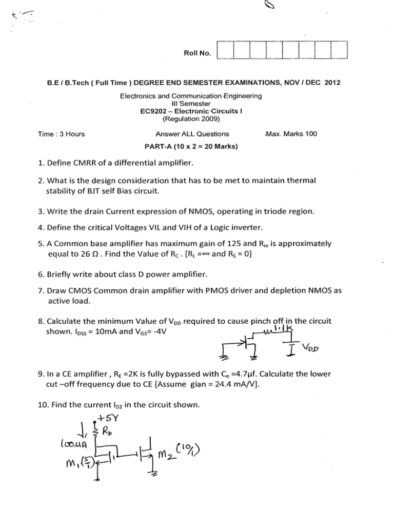
1. Define CMRRof a differential amplifier. 2. What is the design
advertisement

Roll No.
B.E / B.Tech ( Full Time ) D E G R E E END S E M E S T E R EXAMINATIONS, NOV / D E C 2012
Eleqtronics and Communication Engineering
\\\ "Semester
EC9202 - Electronic Circuits I
(ReguJation 2009)
Time : 3 Hours
-Max. Marks 100
Answer ALL Questions
PART-A (10 x 2 = 20 Marks)
1. Define CMRRof a differential amplifier.
2. What is the design consideration that has to be met to maintain thermal
stability of BJT self Bias circuit.
3. Write the drain Current expression of NMOS, operating in triode region.
4. Define the critical Voltages VIL and VIH of a Logic inverter.
5. A Common base amplifier has maximum gain of 125 and R is approximately
equal to 26 Q . Find the Value of R . [R =°° and R = 0]
in
c
L
s
6. Briefly write about class D power amplifier.
7. Draw CMOS Common drain amplifier with PMOS driver and depletion NMOS as
active load.
8. Calculate the minimum Value of V
sh own.
DD
required to cause pinch off in the circuit
IDSS ~
10mA and V =-4V
l t A
GS
2
—
i
T
V DP
,
9. In a CE amplifier, R =2K is fully bypassed with C =4.7u.f. Calculate the lower
c u t - o f f frequency due to CE [Assume gian = 24.4 mA/V].
E
10. Find the current l
(CCUA.PI
D2
e
in the circuit shown.
J
(VI
Part - B ( 5 x 16 = 80 marks)
l l ( i ) Draw a Darlington amplifier and its equivalent circuit. Derive for A , A| , R,
and R .
(10)
(ii) Design a single stage CE amplifier with gain of -29 using Fixed Bias with
y = 15v and R = 10K. & l =0.5mA and h =100
(6)
v s
S
N
0
cc
L
C Q
fe
12(a)(i) Design the Circuit given : l =1.5mA, V =4Vand h =100
c
c
fe
,+-10Y
(6)
1-loV
ii) For the biasing circuit shown , derive expressions for the stability factors
S, S' and S"
rn
^
'
(10)
(OR)
(b) (i) Explain circuits using diodes to compensate for the changes in l
c o
and V
BE
(8)
(ii) For the Circuit given find the maximum peak to peak signal when R = I • 2-^
L
iti—
(8)
13 (a)(i) Draw a MOS differential amplifier with PMOS current source as active
load and derive for its A and A with equivalent circuit.
(10)
(ii)Draw a Current steering circuit with one sink and one source terminal.
Write the expressions for all the terminal currents in terms of the reference
current.
(6)
d
c
(OR)
(b) (i) Draw a CMOS common source amplifier without feedback with NMOS
driver and PMOS diode as active load
(10)
• with equivalent circuit of active load derive for its-offered resistance
• with equivalent circuit of driver,derive for the Voltage gain.
ii) Calculate width of the devices M i and M , Given U = L =1 u.m and
l =120u.A p. c =180u.A/V V = IV and X=0
(6)
2
2
2
D
n
0
tn
A).
14(a) (i)Draw a discrete Common drain amplifier, with its equivalent Circuit
derive for its A , RIN and R .
(8)
(ii) Draw the Voltage transfer curve of CMOS inverter function indicating
the five regions of operation
(4)
(iii) Determine the region of operation of CMOS inverter, when V = 1.1 V
justify your answer. Assume V = 2.5V, V = 0.5, V = - 0.5
(4)
v
0
jn
0 D
tn
tp
(OR)
(b) (i) With Voltage transfer Curve of NMOS inverter. Derive expressions for
Noise margin in High and Low states.
(8)
(ii) Design an NMOS inverter with maximum power dissipation = 0.5mW
u c =25 U.A/V and V =5V . V =0.8V. Draw the load line and mark the
operating point in cut - o f f and triode regions.
(8)
2
n
0
DD
T
15{a) (i) Explain class B power amplifier and derive for its efficiency
(10)
(ii) Design a class A transformer coupled power amplifier to deliver ac
power of 5 watts to a load of 300Q at 30% efficiency, find ac power
across the load and power dissipation. A\so draw the designed circuit.
Assume V =20V and h = 60
(6)
CC
fe
(OR)
15.(b) (i)Define and derive for f and f p.
(8)
a
(ii)For the Circuit shown calculate the midband gain and effective higher cut
-off frequency.
(8)
Rc=9K
hfe =100 Cbott
R =1K
hie =5.2k
Rx=125K
Cb'e=35pf
E
R =50K
2
Cb'c =4pf
R =26K
3
R =100Q
s
& Hi
(8)
TJU)
![1. [50] In the differential amplifier shown below, two resistors are](http://s2.studylib.net/store/data/018291082_1-86a1ae0c6da8478e3f120e87ec3d2b40-300x300.png)
