IS31AP2031
CLASS-G AUDIO POWER AMPLIFIER
WITH INTEGRATED CHARGE PUMP CONVERTER
January 2012
GENERAL DESCRIPTION
FEATURES
The IS31AP2031 is a Class-G audio power amplifier
with automatic gain control. It drives up to 2.0W (10%
THD+N) into an 8Ω speaker from a 4.2V VDD supply.
The IS31AP2031 provides low cost, space saving
solution for portable equipments which need audio
output with higher power by boosting up supply voltage.
Its external components just include a few capacitors
and resistors (no inductor).
The IS31AP2031 use fully differential design to reduce
RF noise. The IS31AP2031 integrates de-pop circuitry to
reduce pop and click noise during power on/off or
shutdown enable operation. The IS31AP2031 also
integrates thermal and short circuit protection function.
Operates from 2.7V to 4.5V
2.0W into an 8Ω load from a 4.2V supply(10%
THD+N)
4 gain levels: 12dB, 16dB, 24dB, 27.5dB
AGC function
Pulse Count Control serial interface
8kV HBM ESD
Thermal and short-circuit protection
Integrated Click-and-Pop suppression circuitry
Available in QFN-20(3mm × 3mm) package
APPLICATIONS
IS31AP2031 is available in QFN-20 (3mm × 3mm)
package. It operates from 2.7V to 4.5V over the
temperature range of -40°C to +85°C.
Smart phones
Cellular phones
PDAs
GPS
Portable electronics
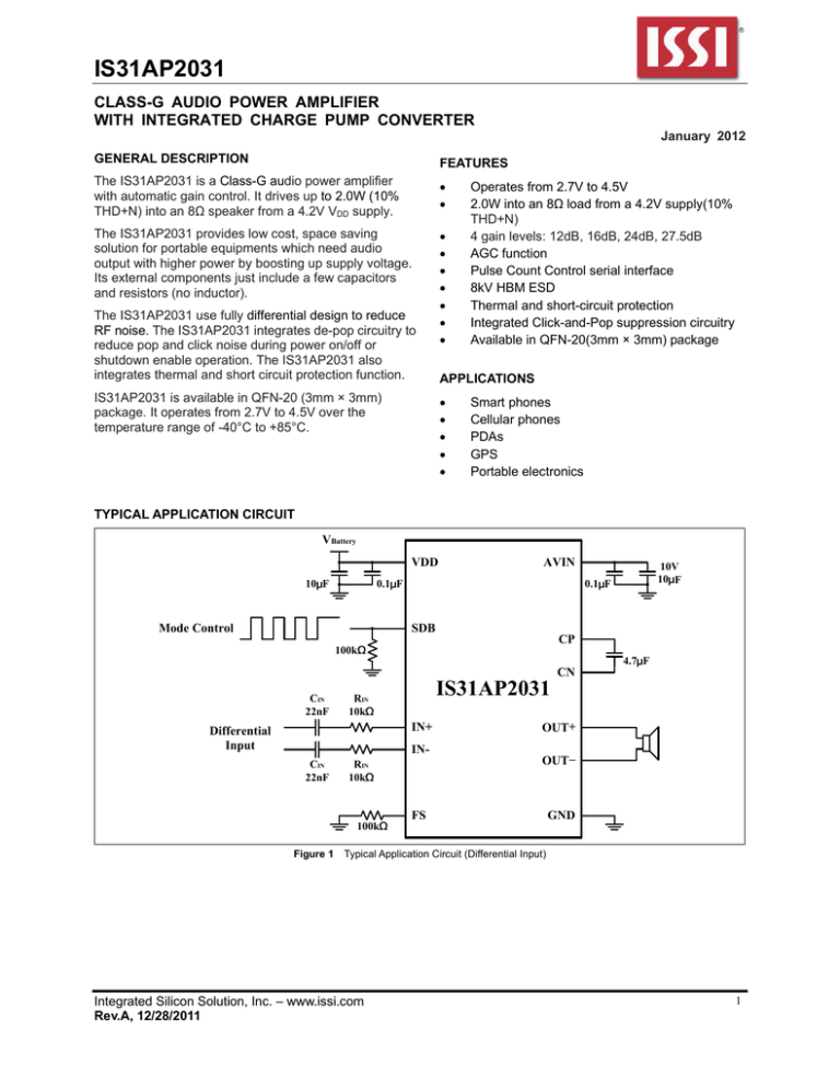
TYPICAL APPLICATION CIRCUIT
VBattery
VDD
10 F
AVIN
0.1 F
Mode Control
10V
10 F
0.1 F
SDB
CP
100k
4.7 F
CN
CIN
22nF
IS31AP2031
RIN
10k
IN+
Differential
Input
OUT
INCIN
22nF
OUT
RIN
10k
FS
GND
100k
Figure 1
Typical Application Circuit (Differential Input)
Integrated Silicon Solution, Inc. – www.issi.com
Rev.A, 12/28/2011
1
IS31AP2031
VBattery
VDD
10 F
AVIN
0.1 F
Mode Control
10V
10 F
0.1 F
SDB
CP
100k
4.7 F
CN
CIN
22nF
IS31AP2031
RIN
10k
IN+
Single-ended
Input
OUT
INCIN
22nF
OUT
RIN
10k
FS
GND
100k
Figure 2
Typical Application Circuit (Single-ended Input)
Integrated Silicon Solution, Inc. – www.issi.com
Rev.A, 12/28/2011
2
IS31AP2031
PIN CONFIGURATION
Package
Pin Configuration (Top View)
QFN-20
PIN DESCRIPTION
No.
Pin
Description
1
SDB
Shutdown pin. Active low.
2,5,10,11,16
NC
No connection.
3
CP
Positive input for external flying cap.
4,8
VDD
Power supply.
6
IN-
Negative audio input.
7
IN+
Positive audio input.
9
FS
Pull 100kΩ resistor to ground.
12,17,18
AVIN
Amplifier supply voltage.
13
OUT-
Negative audio output.
14,20
GND
GND.
15
OUT+
Positive audio output.
19
CN
Negative input for external flying cap.
Thermal Pad
Connect to GND.
Copyright © 2011 Integrated Silicon Solution, Inc. All rights reserved. ISSI reserves the right to make changes to this specification and its products at any time without notice. ISSI assumes no liability arising out of the application or use of any information, products or services described herein. Customers are advised to obtain the latest version of this device specification before relying on any published information and before placing orders for products. Integrated Silicon Solution, Inc. does not recommend the use of any of its products in life support applications where the failure or malfunction of the product can reasonably be expected to cause failure of the life support system or to significantly affect its safety or effectiveness. Products are not authorized for use in such applications unless Integrated Silicon Solution, Inc. receives written assurance to its satisfaction, that: a.) the risk of injury or damage has been minimized; b.) the user assume all such risks; and c.) potential liability of Integrated Silicon Solution, Inc is adequately protected under the circumstances
Integrated Silicon Solution, Inc. – www.issi.com
Rev.A, 12/28/2011
3
IS31AP2031
ORDERING INFORMATION
INDUSTRIAL RANGE: -40°C TO +85°C
Order Part No.
Package
QTY/Reel
IS31AP2031-QFLS2-TR
QFN-20, Lead-free
2500
Integrated Silicon Solution, Inc. – www.issi.com
Rev.A, 12/28/2011
4
IS31AP2031
ABSOLUTE MAXIMUM RATINGS
Supply voltage, VDD
Voltage at any input pin
Maximum junction temperature, TJMAX
Storage temperature range, TSTG
Operating temperature range, TA
ESD (HBM)
-0.3V ~ +6.0V
-0.3V ~ VDD+0.3V
150°C
-65°C ~ +150°C
-40°C ~ +85°C
8kV
Note:
Stresses beyond those listed under “Absolute Maximum Ratings” may cause permanent damage to the device. These are stress ratings only
and functional operation of the device at these or any other condition beyond those indicated in the operational sections of the specifications is
not implied. Exposure to absolute maximum rating conditions for extended periods may affect device reliability.
DC CHARACTERISTICS
TA = 25°C, VDD = 2.7V ~ 4.5V, unless otherwise noted. Typical value are TA = +25°C, VDD = 3.6V.
Symbol Parameter
Condition
VDD
Supply voltage
IDD
Quiescent current
VDD = VAVIN = 3.6V, no load
ISD
Shutdown current
VSDB = 0V
FOSC
Clock frequency
VAVIN
Charge pump output
tON
|VOS|
Min.
Typ.
2.7
Max. Unit
4.5
5
mA
1
No load
Charge pump soft start time
Output offset voltage
V
µA
350
kHz
5.7
V
600
µs
3
mV
Mode 1, Mode 2
30
Mode 3, Mode 4
5
RIN
Input resistor
kΩ
FSW
Switching frequency
VIH
Input logic high voltage
VIL
Input logic low voltage
IIH
Input logic high current
VDD = 5.5V, VI = 5.8V
2.1
µA
IIL
Input logic low current
VDD = 5.5V, VI = 0.3V
0.8
µA
TOTP
Over temperature protection
(Note 1)
150
°C
THYS
Hysteresis temperature
(Note 1)
50
°C
250
kHz
1.4
V
0.4
Integrated Silicon Solution, Inc. – www.issi.com
Rev.A, 12/28/2011
V
5
IS31AP2031
AC CHARACTERISTICS (Note 1)
TA = 25°C, VDD = 3.6V, unless otherwise noted.
Symbol
Po
THD+N
tWU
PSRR
Parameter
Condition
THD+N = 10%, f = 1kHz
RL = 8Ω+33µH
Output power
THD+N = 1%, f = 1kHz
RL = 8Ω+33µH
Min.
Typ.
VDD = 3.6V
1.72
VDD = 4.2V
2.0
VDD = 3.6V
1.38
VDD = 4.2V
1.70
VDD = 3.6V, PO = 0.5W, RL = 8Ω+33µH
Total harmonic distortion f = 1kHz
plus noise
VDD = 4.2V, PO = 1.0W, RL = 8Ω+33µH
f = 1kHz
Max.
W
0.33
%
0.53
Wake-up time from
shutdown
35
Power supply rejection
ratio
Unit
VP-P = 200mV,RL = 8Ω,f = 217Hz
-74
VP-P = 200mV,RL = 8Ω,f = 1kHz
-68
ms
dB
tAT
Attack time
10
ms
tRL
Release time
1.2
s
Amax
Max attenuation gain
-8
dB
tLO
Mode control low time
0.75
10
μs
tHI
Mode control high time
0.75
10
μs
CTRL off
shutdown
150
tOFF
time
for
μs
Note 1: Guaranteed by design.
Integrated Silicon Solution, Inc. – www.issi.com
Rev.A, 12/28/2011
6
IS31AP2031
TYPICAL PERFORMANCE CHARACTERISTICS
20
20
RL = 8Ω+33µH
f = 1kHz
10
THD+N(%)
5
THD+N(%)
RL = 8Ω+33µH
10
2
VDD = 4.2V
1
2
VDD = 4.2V
PO = 1W
1
0.2
VDD = 3.6V
PO = 500mW
0.1
0.5
0.05
0.2
VDD = 3.6V
0.1
10m
0.02
0.01
20m
50m
100m
200m
500m
1
2
3
20
50
100
200
THD+N vs. Output Power
2k
5k
10k 20k
Figure 4
THD+N vs. Frequency
60
+0
VDD = 3.6V, 4.2V
RL = 8Ω+33μH
Input Grounded
50
Efficiency(%)
-20
-40
PSRR(dB)
1k
Frequency(H z)
Output Power(W)
Figure 3
500
-60
-80
40
30
20
10
-100
-120
20
50
100
200
500
1k
2k
5k
0
10k 20k
VDD = 4.2V
RL = 8Ω+33μH
0
0.5
1.5
2
Output Power(W)
Frequency(H z)
Figure 5
1
PSRR vs. Frequency
Efficiency vs. Output Power
Figure 6
70
2.5
RL = 8Ω+33μH
f = 1kHz
60
THD+N = 10%
50
Output Power(W)
Efficiency(%)
2
40
30
1.5
1
THD+N = 1%
20
0.5
10
0
VDD = 3.6V
RL = 8Ω+33μH
0
0.5
1
1.5
0
2.5
3
Efficiency vs. Output Power
Integrated Silicon Solution, Inc. – www.issi.com
Rev.A, 12/28/2011
4
4.5
5
Power Supply(V)
Output Power(W)
Figure 7
3.5
Figure 8
Output Power vs. Power Supply
7
IS31AP2031
APPLICATION INFORMATION
GENERAL DESCRIPTION
The IS31AP2031 is a Class-G audio power amplifier
with an integrated charge pump converter. It consists
of a charge pump and a fully differential audio amplifier.
The operating mode and gain are controlled by Pulse
Count Control (PCC wire) serial interface.
AGC FUNCTION
This is the function to control the output in order to
obtain a maximum output level without distortion when
an excessive input is applied which would otherwise
cause clipping at the differential signal output. That is,
with the AGC function, IS31AP2031 lowers the gain of
the digital amplifier to an appropriate value so as not to
cause clipping at the differential signal output.
The attack time is a time interval that gains falls down
with a big signal input enough. And the release time is
a time from target attenuation to no AGC attenuation.
Assuming no limitation by the power supply, the audio
output signal would be as in Figure 9.
Mode 2. If the SDB pin receives three rising edges, the
IC operates in Mode 3. If the SDB pin receives four
rising edges, the IC operates in Mode 4.
Mode 1—12dB, AGC off.
Mode 2—16dB, AGC on.
Mode 3—24dB, AGC off.
Mode 4—27.5, AGC on.
If the SDB pin is pulled to low last at least 150µs, the
IC will be into shutdown mode.
The gain also can be controlled by the input resistors
RIN.
Mode 1: AV = 160kΩ / (30kΩ+RIN)
Mode 2: AV = 240kΩ/ (30kΩ+RIN)
Mode 3: AV = 240kΩ/ (5kΩ+RIN)
Mode 4: AV = 360kΩ/ (5kΩ+RIN)
Mode 1
SDB
Mode 2
SDB
Figure 9
Assuming no Restriction from Power Supply, the Audio
Output Signal
In normal operation without the AGC, the output is
distorted because of the restriction from power supply,
as shown in Figure 10.
Mode 3
SDB
Mode 4
SDB
tHI
tLO
tOFF
Shutdown
SDB
Figure 12
Figure 10
AGC Function Off
CHARGE PUMP
With the AGC function of SN2145A, the optimum
output power can be obtained along with the minimal
distortion. The Figure 11 shows the outcome of AGC
function.
Attack Time
Figure 11
Operating Mode Control
Release Time
AGC Function On
OPERATING MODE
The operating mode and gain are controlled by Pulse
Count Control (PCC wire) serial interface. The
interface records rising edges of the SDB pin and
decodes them into 4 operating mode (Figure 12).
If the SDB pin is pulled to high, receiving one rising
edge, the IC starts up and operates in Mode 1. If the
SDB pin receives two rising edges, the IC operates in
Integrated Silicon Solution, Inc. – www.issi.com
Rev.A, 12/28/2011
The charge pump converter boosts input supply
voltage (VDD) up to a 5.7V output voltage (VOUT). VOUT
is the supply for the Class-G amplifier.
The charge pump converter only needs three external
components: supply decoupling capacitor, output
bypass capacitor and flying capacitor.
Choose low ESR capacitors to ensure the best
operating performance and place the capacitors as
close as possible to the IS31AP2031.
FULLY DIFFERENTIAL AUDIO AMPLIFIER
The fully differential amplifier consists of a differential
amplifier and a common-mode amplifier. The
differential amplifier ensures that the amplifier outputs
a differential voltage on the output that is equal to the
differential input times the gain. The common-mode
feedback ensures that the common-mode voltage at
the output is biased around VDD/2 regardless of the
common-mode voltage at the input.
8
IS31AP2031
The fully differential IS31AP2031 can still be used with
a single-ended input; however, the IS31AP2031
should be used with differential inputs when in a noisy
environment, like a wireless handset, to ensure
maximum noise rejection.
ADVANTAGES OF FULLY DIFFERENTIAL
AMPLIFIERS
The fully differential amplifier does not require a
bypass capacitor. This is because any shift in the
mid-supply affects both positive and negative channels
equally and cancels at the differential output.
GSM handsets save power by turning on and shutting
off the RF transmitter at a rate of 217Hz. The
transmitted signal is picked-up on input and output
traces. The fully differential amplifier cancels the noise
signal much better than the typical audio amplifier.
INPUT CAPACITORS (CIN)
The input capacitors and input resistors form a
high-pass filter with the corner frequency, fC,
determined in Equation (1) when IS31AP2031
operates in Mode 1 and Mode 2.
1
f
c 2 ( R 30k )C
IN
IN
(1)
DESIGN NOTE
COMPONENT SELECTION
The value and ESR of the output capacitor for charge
pump will affect output ripple and transient
performance. A X7R or X5R ceramic capacitor in 10μF
should be recommended. The flying capacitor should
use a 4.7µF X7R or X5R ceramic capacitor.
All the capacitors should support at least 10V.
PCB LAYOUT
The decoupling capacitors should be placed close to
the VDD pin and the output capacitors should be
placed close to the AVIN pin. The flying capacitor
should be placed close to the CN and CP pins. The
input capacitors and input resistors should be placed
close to the IN+ and IN- pins and the traces must be
parallel to prevent noise. The traces of OUT+ and
OUT- pins connected to the speaker should be as
possible as short and wide. The recommended width is
0.5mm.
Trace width should be at least 0.75mm when the
current reaches 1A. Trace width should be at least
1.0mm for the power supply and the ground plane. The
thermal pad and the GND pin should connect directly
to a strong common ground plane for heat sinking.
Follow the Equation (2) when IS31AP2031 operates in
Mode 3 and Mode 4.
1
f
c 2 ( R 5k )C
IN
IN
(2)
The value of the input capacitor is important to
consider as it directly affects the bass (low frequency)
performance of the circuit. Speakers in wireless
phones cannot usually respond well to low frequencies,
so the corner frequency can be set to block low
frequencies in this application.
If the corner frequency is within the audio band, the
capacitors should have a tolerance of 10% or better,
because any mismatch in capacitance causes an
impedance mismatch at the corner frequency and
below.
Integrated Silicon Solution, Inc. – www.issi.com
Rev.A, 12/28/2011
9
IS31AP2031
CLASSIFICATION REFLOW PROFILES
Profile Feature
Pb-Free Assembly
Preheat & Soak
Temperature min (Tsmin)
Temperature max (Tsmax)
Time (Tsmin to Tsmax) (ts)
150°C
200°C
60-120 seconds
Average ramp-up rate (Tsmax to Tp)
3°C/second max.
Liquidous temperature (TL)
Time at liquidous (tL)
217°C
60-150 seconds
Peak package body temperature (Tp)*
Max 260°C
Time (tp)** within 5°C of the specified
classification temperature (Tc)
Max 30 seconds
Average ramp-down rate (Tp to Tsmax)
6°C/second max.
Time 25°C to peak temperature
8 minutes max.
Figure 13
Classification Profile
Integrated Silicon Solution, Inc. – www.issi.com
Rev.A, 12/28/2011
10
IS31AP2031
TAPE AND REEL INFORMATION
Integrated Silicon Solution, Inc. – www.issi.com
Rev.A, 12/28/2011
11
IS31AP2031
PACKAGE INFORMATION
QFN-20
Note: All dimensions in millimeters unless otherwise stated.
Integrated Silicon Solution, Inc. – www.issi.com
Rev.A, 12/28/2011
12
