SG1524/SG2524/SG3524
Regulating Pulse Width Modulator
Description
Features
This monolithic integrated circuit contains all the control
circuitry for a regulating power supply inverter or switching
regulator. Included in a 16-pin dual-in-line package is the
voltage reference, error amplifier, oscillator, pulse width
modulator, pulse steering flip-flop, dual alternating output
switches and current limiting and shut-down circuitry. This
device can be used for switching regulators of either
polarity, transformer coupled DC to DC converters,
transformerless voltage doublers and polarity converters, as
well as other power applications. The SG1524 is specified
for operation over the full military ambient temperature
range of -55°C to +125°C, the SG2524 for -25°C to +85°C,
and the SG3524 is designed for commercial applications of
0°C to +70°C.
8V to 40V Operation
5V Reference
Reference Line and Load Regulation of 0.4%
100Hz to 300kHz Oscillator Range
Excellent External Sync Capability
Dual 50mA Output Transistors
Current Limit Circuitry
Complete PWM Power Control Circuitry
Single Ended or Push-Pull Outputs
Total Supply Current less than 10mA
High Reliability Features
Following are the high reliability features of SG1524:
Block Diagram
Available to MIL-STD-883, ¶ 1.2.1
MIL-M38510/12601BEA SG1524J-JAN
MSC-AMS Level “S” Processing Available
Available to DSCC - Standard Microcircuit
Drawing (SMD)
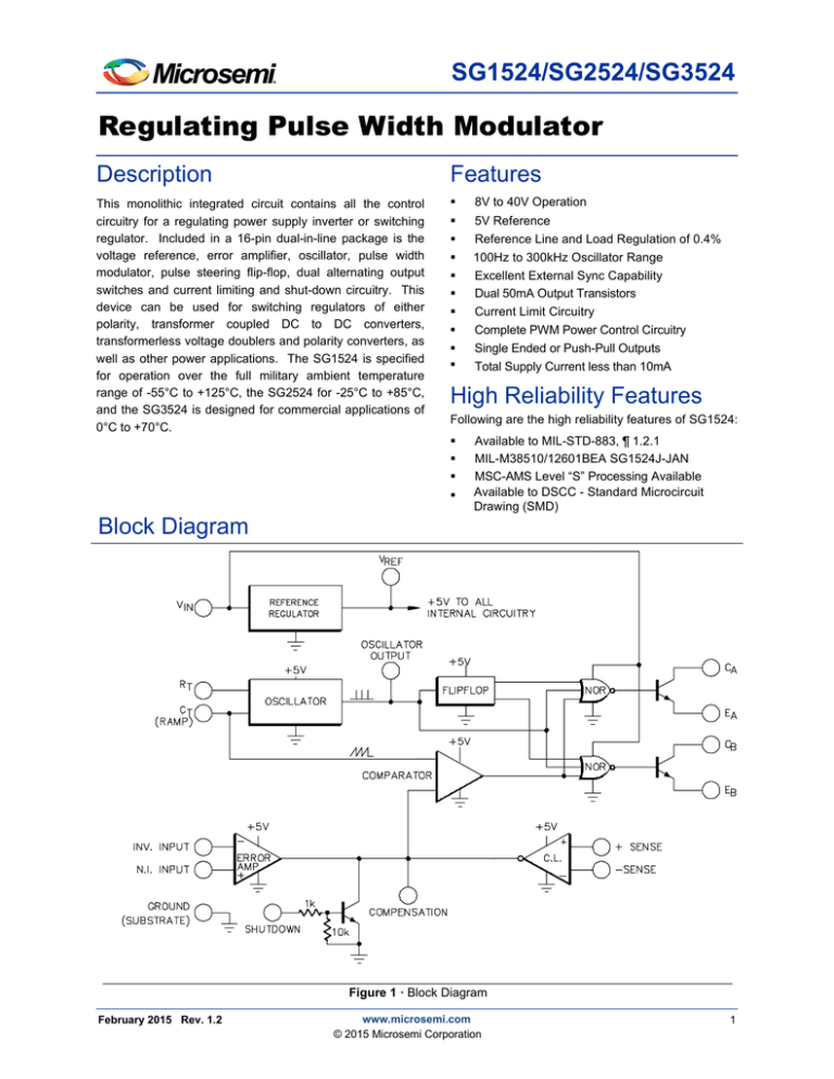
Figure 1 · Block Diagram
February 2015 Rev. 1.2
www.microsemi.com
© 2015 Microsemi Corporation
1
Absolute Maximum Ratings (Note 1)
Input Voltage (+VIN ) ............................................................. 42V
Collector Voltage ................................................................ 40V
Logic Inputs ........................................................... -0.3V to 5.5V
Current Limit Sense Inputs ................................... -0.3V to 0.3V
Output Current (each transistor) .................................... 100mA
Reference Load Current .................................................. 50mA
Oscillator Charging Current ................................................ 5mA
Operating Junction Temperature
Hermetic (J, L Packages) ................................................. 150°C
Plastic (N, D Packages) ................................................... 150°C
Storage Temperature Range ..............................-65°C to 150°C
Lead Temperature (Soldering, 10 seconds).....................300°C
Note 1: Values beyond which damage may occur.
Pb-free / RoHS Peak Package Solder Reflow Temp (40 sec. max.
exposure)... 260°C (+0, -5)
Thermal Data
J Package:
Thermal Resistance-Junction to Case, θJC ............... 30°C/W
Thermal Resistance-Junction to Ambient, θJA ........... 80°C/W
N Package:
Thermal Resistance-Junction to Case, θJC ............... 40°C/W
Thermal Resistance-Junction to Ambient, θJA ........... 65°C/W
D Package:
Thermal Resistance-Junction to Case, θJC ............... 50°C/W
Thermal Resistance-Junction to Ambient, θJA ......... 120°C/W
L Package:
Thermal Resistance-Junction to Case, θJC ........... .... 35°C/W
Thermal Resistance-Junction to Ambient, θJA ......... 120°C/W
Note A. Junction Temperature Calculation: TJ = TA + (PD x θJA).
Note B. The above numbers for θJC are maximums for the limiting
thermal resistance of the package in a standard mounting
configuration. The θJA numbers are meant to be
guidelines for the thermal performance of the device/pcboard system. All of the above assume no ambient
airflow.
Recommended Operating Conditions (Note 2)
Input Voltage (+VIN) ................................................... 8V to 40V
Collector Voltage ....................................................... 0V to 40V
Error Amp Common Mode Range ..........................1.8V to 3.4V
Current Limit Sense Common Mode Range ........ -0.3V to 0.3V
Output Current (each transistor) ............................... 0 to 50mA
Reference Load Current ........................................... 0 to 20mA
Oscillator Charging Current .................................. 30µA to 2mA
Oscillator Frequency Range ......................... 100Hz to 300kHz
Oscillator Timing Resistor (RT) ........................ 1.8kΩ to 100kΩ
Oscillator Timing Capacitor (CT) ............................ 1nF to 1.0µF
Operating Ambient Temperature Range
SG1524 ......................................................... -55°C to 125°C
SG2524 ........................................................... -25°C to 85°C
SG3524 ............................................................... 0°C to 70°C
Note 2: Range over which the device is functional and parameter limits are guaranteed.
Electrical Characteristics
(Unless otherwise specified, these specifications apply over the operating ambient temperatures for SG1524 with -55°C ≤ TA ≤ 125°C, SG2524 with
-25°C ≤ TA ≤ 85°C, SG3524 with 0°C ≤ TA ≤ 70°C, and +V IN = 20V. Low duty cycle pulse testing techniques are used which maintains junction and
case temperatures equal to the ambient temperature.)
Parameter
Reference Section (Note 3)
Output Voltage
Line Regulation
Load Regulation
Temperature Stability (Note 7) Total
Output Voltage Range (Note 7)
Short Circuit Current
Test Conditions
TJ = 25°C
VIN = 8V to 40V
IL = 0 to 20mA
Over Operating Temperature Range
Over Line, Load and Temperature
VREF = 0V
Note 3. IL = 0mA
2
SG1524/SG2524
SG3524
Units
Min. Typ. Max. Min. Typ. Max.
4.80 5.00 5.20 4.60 5.00 5.40
20
30
50
50
50
50
4.80
5.20 4.60
5.40
25
50 150 25
50 150
V
mV
mV
mV
V
mA
Electrical Characteristics (Continued)
Parameter
Oscillator Section (Note 4)
Initial Accuracy
Voltage Stability
Maximum Frequency
Sawtooth Peak Voltage
Sawtooth Valley Voltage
Clock Amplitude
Clock Pulse Width
Error Amplifier Section (Note 5)
Input Offset Voltage
Input Bias Current
Input Offset Current
DC Open Loop Gain
Output Low Level
Output High Level
Common Mode Rejection
Supply Voltage Rejection
Gain-Bandwidth Product (Note 7)
P.W.M. Comparator (Note 4)
Minimum Duty Cycle
Maximum Duty Cycle
Test Conditions
TJ = 25°C
MIN ≤ TJ ≤ MAX
VIN = 8V to 40V
RT = 2kΩ, CT = 1nF
VIN = 40V
VIN = 8V
36
34
200
3
0.6
3.2
0.3
RS ≤ 2kΩ
40
0.1
400
1
44
46
1
3.8
1.2
1.5
0.5
1
5
10
1
0.2
4.2
0.5
36
34
200
3
0.6
3.2
0.3
0.1
400
1
3.8
1.2
1.5
0.2
4.2
0.5
3.8
1
2
45
49
VCOMP = 0.5V
VCOMP = 3.6V
45
49
190
200
210
200
180
0.5
0.2
0.8
1.2
1.8
0.5
0.2
60
2
200
220
200
mV
µA
0.8
1.2
1.8
V
V
50
2
0.4
0.2
µA
V
V
µs
µs
10
mA
17
0.4
0.2
7
10
mV
µA
µA
dB
V
V
dB
dB
MHz
%
%
50
2
17
kHz
kHz
%
kHz
V
V
V
µs
0
0
7
FOSC = 40kHz (RT = 2.9kΩ, CT = .01µF)
VCM = 2.5V
VCM = 0V
These parameters, although guaranteed over the recommended operating conditions, are not 100% tested in production.
3
44
46
1
10
10
2
3.8
70
55
1
72
40
2
1
RL ≥10MΩ, TJ = 25°C
VPIN 1 - VPIN 2 ≥ 150mV
VPIN 2 - VPIN 1 ≥150mV
VCM = 1.8V to 3.4V
VIN = 8V to 40V
TJ = 25°C
Current Limit Amplifier Section (Note 6)
TJ = 25°C
Sense Voltage
Input Bias Current
Shutdown Section
Threshold Voltage
TJ = 25°C
MIN ≤ TJ ≤ MAX
Output Section (each transistor)
Collector Leakage Current
VCE = 40V
Collector Saturation Voltage
IC = 50mA
Emitter Output Voltage
IE = 50mA
RC = 2kΩ
Collector Voltage Rise Time
Collector Voltage Fall Time
RC = 2kΩ
Power Consumption
Standby Current
VIN = 40V
Note 4.
Note 5.
Note 6.
Note 7.
SG3524
SG1524/SG2524
Units
Min. Typ. Max. Min. Typ. Max.
Application Notes
OSCILLATOR
The oscillator in the SG1524 uses an external resistor RT to
establish a constant charging current into an external capacitor
CT. While this uses more current than a series-connected RC, it
provides a linear ramp voltage at CT which is used as a timedependent reference for the PWM comparator. The charging
current is equal to 3.6V/RT, and should be restricted to between
30µA and 2mA. The equivalent range for RT is 100k to 1.8k.
Note that for buck regulator topologies, the two outputs can be
wire-ORed for an effective 0-90% duty cycle range. With this
connection, the output frequency is the same as the oscillator
frequency. For push-pull applications, the outputs are used
separately; the flip-flop limits the duty cycle range at each output
to 0-45%, and the effective switching frequency at the transformer is 1/2 the oscillator frequency.
The range of values for CT also has limits, as the discharge time
of CT determines the pulse width of the oscillator output pulse.
The pulse is used (among other things) as a blanking pulse to
both outputs to insure that there is no possibility of having both
outputs on simultaneously during transitions. This output
deadtime relationship is shown in Figure 2. A pulse width below
0.35 microseconds may cause failure of the internal flip-flop to
toggle. This restricts the minimum value of CT to 1000pF. (Note:
Although the oscillator output is a convenient oscilloscope sync
input, the probe capacitance will increase the pulse width and
decrease the oscillator frequency slightly.) Obviously, the upper
limit to the pulse width is determined by the modulation range
required in the power supply at the chosen switching frequency.
Practical values of CT fall between 1000pF and 0.1µF, although
successful 120 Hz oscillators have been implemented with
values up to 5µF and a series surge limit resistor of 100 ohms.
If it is desired to synchronize the SG1524 to an external clock, a
positive pulse may be applied to the clock pin. The oscillator
should be programmed with RT and CT values that cause it to
free-run at 90% of the external sync frequency. A sync pulse
with a maximum logic 0 of +0.3 volts and a minimum logic 1 of
+2.4 volts applied to Pin 3 will lock the oscillator to the external
source. The minimum sync pulsewidth should be 200
nanoseconds, and the maximum is determined by the required
deadtime. The clock pin should never be driven more negative
than -0.3 volts, nor more positive than +5.0 volts. The
nominal resistance to ground is 3.2k at the clock pin, ±25%
over temperature.
If two or more SG1524's must be synchronized together, program
one master unit with RT and CT for the desired frequency.
Leave the RT pins on the slaves open, connect the CT pins to
the CT of the master, and connect the clock pins to the clock pin
of the master. Since CT is a high-impedance node, this sync
technique works best when all devices are close together.
The oscillator frequency is approximately 1/RT•CT; where R is in
ohms, C is in microfarads, and the frequency is in Megahertz.
For greater accuracy, the chart in Figure 3 may be used for a
wide range of operating frequencies.
20
100k
10
50k
5
20k
2
10k
1
5k
0.5
2k
1k
0.2
.001
.002
.005
.01
.02
.05
500
0.1
1k
2k
5k
10k
20k
50k 100k
200k 500k
Figure 3 · Oscillator Frequency vs. RT and CT
Figure 2 · Output Stage Deadtime vs. CT
4
Application Notes (Continued)
CURRENT LIMITING
The current limiting circuitry of the SG1524 is shown in Figure 4.
By matching the base-emitter voltages of Q1 and Q2, and
assuming a negligible voltage drop across R1:
A second factor to consider is that the response time is
relatively slow. The current limit amplifier is internally
compensated by R1, C1, and Q1, resulting in a roll-off pole at
approximately 300 Hz. A third factor to consider is the bias
current of the C.L. sense pins. A constant current of
approximately 150µA flows out of Pin 4, and a variable current
with a range of 0-150µA flows out of Pin 5. As a result, the
equivalent source impedance seen by the current sense pins
should be less than 50 ohms to keep the threshold error less
than 5%.
C.L. Threshold = VBE(Q1) + I1• R2 - VBE(Q2) = I1• R 2
~ 200 mV
Although this circuit provides a relatively small threshold with a
negligible temperature coefficient, there are some limitations to
its use because of its simplicity.
Since the gain of this circuit is relatively low (42 dB), there is a
transition region as the current limit amplifier takes over pulse
width control from the error amplifier. For testing purposes,
threshold is defined as the input voltage required to get 25% duty
cycle (+2 volts at the error amplifier output) with the error amplifier
signaling maximum duty cycle.
The most important of these is the limited common-mode voltage
range: ±0.3 volts around ground. This requires sensing in the
ground or return line of the power supply. Also precautions
should be taken to not turn on the parasitic substrate diode of the
integrated circuit, even under transient conditions. A Schottky
clamp diode at Pin 5 may be required in some configurations to
achieve this.
APPLICATION NOTE: If the current limit function is not used on
the SG1524, the common-mode voltage range restriction requires both current sense pins to be grounded.
Figure 4 · Current Limiting Circuitry of the SG1524
5k
5k
5k
5k
1k
1k
5k
5k
5k
5k
2k
1k
1k
2k
3k
20k
50k
In this conventional single-ended regulator circuit, the two outputs of the SG1524 are connected in parallel for effective 0 - 90%
duty-cycle modulation. The use of an output inductor requires
and R-C phase compensation network for loop stability.
Push-pull outputs are used in this transformer-coupled DC-DC
regulating converter. Note that the oscillator must be set at twice
the desired output frequency as the SG1524's internal flip-flop
divides the frequency by 2 as it switches the PWM signal from
one output to the other. Current limiting is done here in the
primary so that the pulse width will be reduced should transformer
saturation occur.
5
Connection Diagrams and Ordering Information (See Notes Below)
Package
16-PIN CERAMIC DIP
J - PACKAGE
Part No.
SG1524J-883B
SG1524J-JAN
SG1524J-DESC
SG1524J
SG2524J
SG3524J
Ambient
Temperature Range
-55°C to 125°C
-55°C to 125°C
-55°C to 125°C
-55°C to 125°C
-25°C to 85°C
0°C to 70°C
16-PIN PLASTIC DIP
N - PACKAGE
SG2524N
SG3524N
-25°C to 85°C
16-PIN NARROW BODY
PLASTIC SOIC
D - PACKAGE
SG2524D
SG3524D
-25°C to 85°C
0°C to 70°C
0°C to 70°C
Connection Diagram
INV. INPUT
N.I. INPUT
OSC. OUTPUT
+C.L. SENSE
-C.L. SENSE
RT
CT
GROUND
1
16
2
15
3
14
4
13
5
12
6
11
7
10
8
9
VREF
+VIN
EB
CB
CA
EA
SHUTDOWN
COMPENSATION
N Package: RoHS / Pb-free Transition DC: 0503*. 100% Matte Tin Lead Finish
INV. INPUT
N.I. INPUT
OSC. OUTPUT
+C.L. SENSE
-C.L. SENSE
RT
1
16
2
15
3
14
4
13
5
12
6
11
CT
7
10
GROUND
8
9
VREF
+VIN
EB
CB
CA
EA
SHUTDOWN
COMPENSATION
RoHS / Pb-free transition DC:0440
Pb-free / RoHS 100% Matte Tin Lead Finish*
20-PIN CERAMIC
LEADLESS CHIP CARRIER
L- PACKAGE
SG1524L-883B
SG1524L
-55°C to 125°C
-55°C to 125°C
3
1. N.C.
2. VREF
3. INV. INPUT
4. N.I. INPUT
5. OSC. OUTPUT
6. + C.L. SENSE
7. - C.L. SENSE
8. RT
9. CT
10. GROUND
2
1
20 19
4
18
5
17
6
16
7
15
8
14
9
10 11 12 13
*RoHS compliant
Note 1. Contact factory for JAN product availablity.
2. All packages are viewed from the top.
3. Hermetic Packages J & L use Pb37/Sn63 hot solder lead finish, contact factory for availability of RoHS versions.
6
11. COMP
12. SHUTDOWN
13. N.C.
14. EA
15. CA
16. N.C.
17. CB
18. EB
19. N.C.
20. +VIN
Package Outline Dimensions
Package Outline Dimensions
Controlling dimensions are in inches, metric equivalents are shown for general information.
DIM
D
16
9
1
8
A
b
b2
c
D
E
e
eA
H
L
θ
Q
E
eA
b2
Q A
Seating Plane
L c
H
θ
b
e
MILLIMETERS
MIN
MAX
5.08
0.38
0.51
1.04
1.65
0.20
0.38
19.30
19.94
5.59
7.11
2.54 BSC
7.37
7.87
0.63
1.78
3.18
5.08
15°
0.51
1.02
INCHES
MIN
MAX
0.200
0.015
0.020
0.045
0.065
0.008
0.015
0.760
0.785
0.220
0.280
0.100 BSC
0.290
0.310
0.025
0.070
0.125
0.200
15°
0.020
0.040
Note:
Dimensions do not include protrusions; these shall not
exceed 0.155mm (.006”) on any side. Lead dimension
shall not include solder coverage.
Figure 5 · J 16-Pin Ceramic Dip
DIM
D
MIN
MAX
A
-
A1
0.38
A2
E1
1
b1
E
A
c
A1
L
e
b
SEATING PLANE
θ
INCHES
MIN
MAX
5.33
-
0.210
-
0.015
3.30 Typ.
-
0.130 Typ.
b
0.36
0.56
0.014
0.022
b1
1.14
1.78
0.045
0.070
c
0.20
0.36
0.008
0.014
D
18.67
19.69
0.735
0.775
e
A2
MILLIMETERS
2.54 BSC
0.100 BSC
E
7.62
8.26
0.300
0.325
E1
6.10
7.11
0.240
0.280
L
2.92
0.381
0.115
0.150
θ
-
15°
-
15°
Note:
Dimensions do not include protrusions; these shall not
exceed 0.155mm (.006”) on any side. Lead dimension
shall not include solder coverage.
Figure 6 · N 16-Pin Plastic Dual Inline Package Dimensions
7
Package Outline Dimensions(continued)
DIM
A
A1
A2
b
c
D
E
e
H
L
Θ
*LC
MILLIMETERS
MIN
MAX
1.35
1.75
0.10
0.25
1.25
1.52
0.33
0.51
0.19
0.25
9.78
10.01
5.79
6.20
1.27 BSC
3.81
4.01
0.40
1.27
0
8
0.10
INCHES
MIN
MAX
0.053
0.069
0.004
0.010
0.049
0.060
0.013
0.020
0.007
0.010
0.385
0.394
0.228
0.244
0.050 BSC
0.150
0.158
0.016
0.050
0
8
0.004
*Lead Coplanarity
Note:
Dimensions do not include mold flash or protrusions;
these shall not exceed 0.155mm (.006”) on any side.
Lead dimension shall not include solder coverage.
Figure 7 · D 16-Pin Plastic SOIC
E3
D
DIM
E
A
A1
L2
3
8.64
9.14
0.340
0.360
E3
-
8.128
-
0.320
e
1.270 BSC
0.050 BSC
B1
0.635 TYP
0.025 TYP
L
1.02
1.52
0.040
0.060
A
1.626
2.286
0.064
0.090
1.016 TYP
1.372
1.68
0.054
0.066
A2
-
1.168
-
0.046
L2
1.91
2.41
0.075
0.203R
13
h
B1
e
0.95
0.008R
Note:
All exposed metalized area shall be gold plated 60 microinch minimum thickness over nickel plated unless
otherwise specified in purchase order.
1
18
0.040 TYP
A1
B3
A2
INCHES
MIN
MAX
D/E
h
L
8
MILLIMETERS
MIN
MAX
B3
Figure 8 · L 20-Pin Ceramic LCC Package Outline Dimensions
8
Microsemi Corporation (Nasdaq: MSCC) offers a comprehensive portfolio of semiconductor
and system solutions for communications, defense & security, aerospace and industrial
markets. Products include high-performance and radiation-hardened analog mixed-signal
integrated circuits, FPGAs, SoCs and ASICs; power management products; timing and
synchronization devices and precise time solutions, setting the world’s standard for time; voice
processing devices; RF solutions; discrete components; security technologies and scalable
anti-tamper products; Power-over-Ethernet ICs and midspans; as well as custom design
capabilities and services. Microsemi is headquartered in Aliso Viejo, Calif., and has
approximately 3,400 employees globally. Learn more at www.microsemi.com.
Microsemi Corporate Headquarters
One Enterprise, Aliso Viejo,
CA 92656 USA
Within the USA: +1 (800) 713-4113
Outside the USA: +1 (949) 380-6100
Sales: +1 (949) 380-6136
Fax: +1 (949) 215-4996
E-mail: sales.support@microsemi.com
© 2015 Microsemi Corporation. All
rights reserved. Microsemi and the
Microsemi logo are trademarks of
Microsemi Corporation. All other
trademarks and service marks are the
property of their respective owners.
Microsemi makes no warranty, representation, or guarantee regarding the information contained herein or
the suitability of its products and services for any particular purpose, nor does Microsemi assume any
liability whatsoever arising out of the application or use of any product or circuit. The products sold
hereunder and any other products sold by Microsemi have been subject to limited testing and should not
be used in conjunction with mission-critical equipment or applications. Any performance specifications are
believed to be reliable but are not verified, and Buyer must conduct and complete all performance and
other testing of the products, alone and together with, or installed in, any end-products. Buyer shall not rely
on any data and performance specifications or parameters provided by Microsemi. It is the Buyer's
responsibility to independently determine suitability of any products and to test and verify the same. The
information provided by Microsemi hereunder is provided "as is, where is" and with all faults, and the entire
risk associated with such information is entirely with the Buyer. Microsemi does not grant, explicitly or
implicitly, to any party any patent rights, licenses, or any other IP rights, whether with regard to such
information itself or anything described by such information. Information provided in this document is
proprietary to Microsemi, and Microsemi reserves the right to make any changes to the information in this
document or to any products and services at any time without notice.
SG1524.1.2/02.15
