AGC Lab: Automatic Gain Control Circuits
advertisement

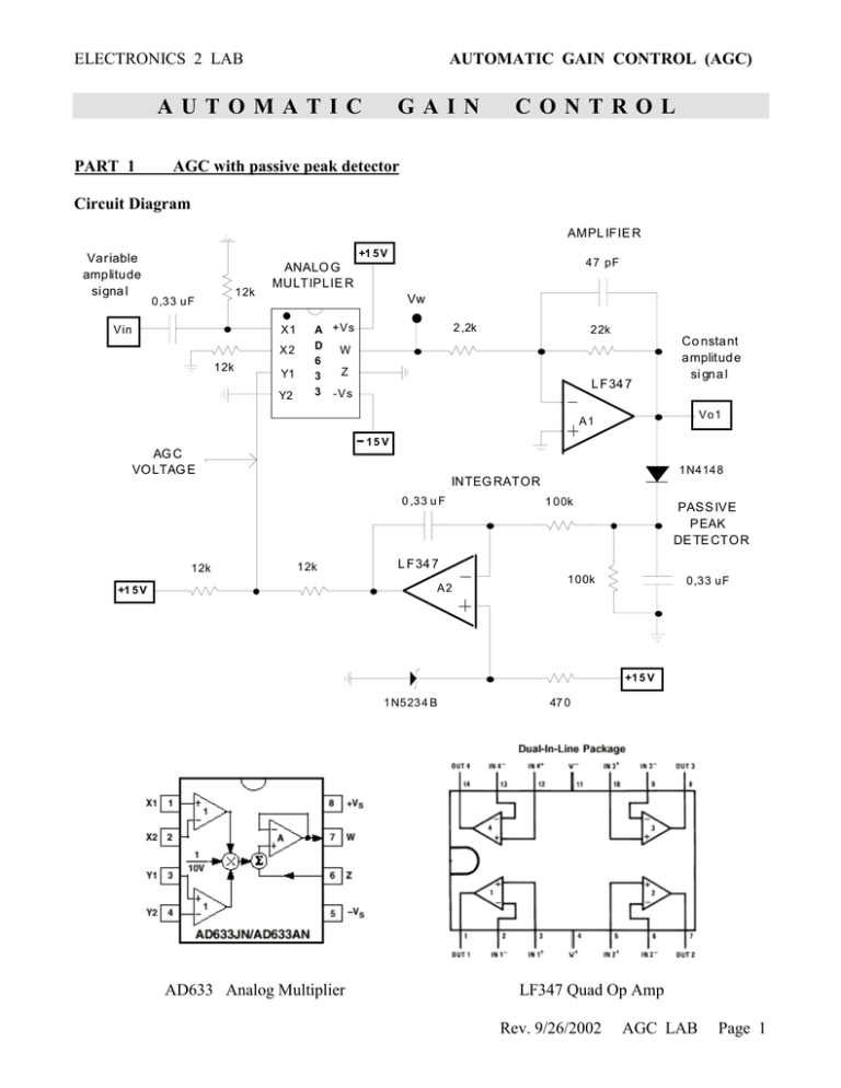
ELECTRONICS 2 LAB AUTOMATIC GAIN CONTROL (AGC) AUTOMATIC PART 1 GAIN CONTROL AGC with passive peak detector Circuit Diagram AMPL IFIE R Var iable amplitude si gna l +1 5 V 12k 0,33 uF V in Vw X1 X2 12k 47 pF ANALO G MULTIPL IE R Y1 Y2 2 ,2k A +V s D W 6 Z 3 3 -V s 22k L F34 7 Co nsta nt amplitud e si gna l V o1 A1 15 V AG C VOLTAG E 1N414 8 INTEG RATOR 0 ,33 u F 12k 12k PASS IVE PEAK DE TE CTOR L F34 7 A2 +1 5 V 1 00k 100k 0,33 uF +1 5 V 1N523 4 B AD633 Analog Multiplier 47 0 LF347 Quad Op Amp Rev. 9/26/2002 AGC LAB Page 1 ELECTRONICS 2 LAB AUTOMATIC GAIN CONTROL (AGC) Pre-lab 1. Determine the regulated amplitude of Vo1 – look up Zener data at http://www.fairchildsemi.com/ 2. Determine VY1 min and max assuming typical saturation voltages for LF347 with Vsup = ±15V 3. Determine the range of input voltages (main input Vin) for which the AGC is operational. Why does not the AGC work outside this above-calculated range? 4. What is the peak AC voltage of Vw? 5. Determine the peak to peak ripple at the peak detector output and at VY1 for frequencies of 1 kHz and 10 kHz. Draw the expected ripple waveforms. Lab Procedure NOTE: 1. The HP signal generator displays half the actual O/P amplitude if load >> 50Ω If load = 50Ω, it displays the correct amplitude. Assemble circuit as per breadboard layout provided at the end. 2. Using a 1 kHz input sinewave, adjust the amplitude of Vin in order to obtain the DC voltages for VY1 listed below. For each case measure the corresponding values of Vo2 (DC), Vo1 (rms), Vw(rms) and Vin (rms) with the DMM. Monitor Vin and Vo1 on the oscilloscope throughout. Calculate Amult from measurements. 3. Repeat the above for VY1(DC) slightly above minimum and slightly below maximum when Vo1 is still constant. VY1 (DC) min 1 2 4 6 8 10 max Vo2 (DC) Vo1 (rms) Vin (rms) Vw(rms) A mult = 4. Vw Vin Measure the exact value of the Zener reference voltage – record value. 5. Measure the ripple voltage (with the scope) at the peak detector output and at VY1 at frequencies of 100 Hz, 1 kHz and 10 kHz – ripple may be too small to be measured in some cases. Ensure that Vin is within operating range. Rev. 9/26/2002 AGC LAB Page 2 ELECTRONICS 2 LAB AUTOMATIC GAIN CONTROL (AGC) 6. With Vin set such as to obtain VY1 around 4V DC, measure Vo1 (rms) at 1 kHz, 10 kHz, 100 kHz and measure the minimum and maximum frequencies at which Vo1 is no longer regulated. 7. Measure THD of Vin, Vw and Vo1 at 1 kHz when AGC loop functions at VY1 = 1V and VY1=10V. %THD of Vw %THD of Vin %THD of Vo1 VY1 = 1V VY1 = 10V Post lab 1. Compare measured values to pre-lab values everywhere applicable. 2. Did Vo1 vary at all? What was the % variation of Vo1 over the entire range of Vin at 1 kHz? Is this % variation acceptable? Explain. 3. Which device introduced the most distortion? Explain. Was distortion different for different input levels? 4. Using the results of step 3 of the procedure, explain how the AGC circuit works. PART 2 AGC with active peak detector Circuit Diagram Va ria ble am plitu de sig na l +1 5V 12k 0,33 uF V in ANALO G MUL TIPLIER X1 X2 12k AMPLIFIER Vw Y1 Y2 2 ,2k A +Vs D W 6 Z 3 3 -V s 22k V o1 LF3 47 C on sta nt am p litude sig na l A1 1 5V AGC VO LTAGE 12 k AC TIVE PEAK DETEC TO R INT EGR ATO R 0,3 3 uF 12k 100k 1 2K LF3 47 1N4 148 A4 A2 +1 5V A3 +15 V 1 N 52 34B 100K 0,33 uF 47 0 Pre-lab Rev. 9/26/2002 AGC LAB Page 3 ELECTRONICS 2 LAB AUTOMATIC GAIN CONTROL (AGC) 1. Determine the regulated amplitude of Vo1 – look up Zener data at http://www.fairchildsemi.com/ 2. Determine VY1 min and max assuming typical saturation voltages for LF347 with Vsup = ±15V 3. Determine the range of input voltages (main input Vin) for which the AGC is operational. Why does not the AGC work outside this above-calculated range? 4. What is the peak AC voltage of Vw? 5. Determine the peak to peak ripple at the peak detector output and at VY1 for frequencies of 1 kHz and 10 kHz. Draw the expected ripple waveforms. Lab Procedure 1. Assemble circuit as per breadboard layout provided at the end – don’t forget to remove the 47 pF capacitor in the inverting amplifier. 2. Using a 1 kHz input sinewave, adjust the amplitude of Vin in order to obtain the DC voltages for VY1 listed below. For each case measure the corresponding values of Vo2 (DC), Vo1 (rms), Vw(rms) and Vin (rms) with the DMM. Monitor Vin and Vo1 on the oscilloscope throughout. Calculate Amult from measurements. 3. Repeat the above for VY1(DC) slightly above minimum and slightly below maximum when Vo1m is still constant. VY1 (DC) min 1 5 10 max Vo2 (DC) Vo1 (rms) Vin (rms) Vw(rms) A mult = 4. Vw Vin Measure the exact value of the Zener reference voltage – record value. 5. Measure the ripple voltage (with the scope) at the peak detector output and at VY1 at frequencies of 100 Hz, 1 kHz and 10 kHz – ripple may be too small to be measured in some cases. Ensure that Vin is within operating range. 6. With Vin set such as to obtain VY1 around 4V DC, measure Vo1 (rms) at 1 kHz, 10 kHz, 100 kHz and measure the minimum and maximum frequencies at which Vo1 is no longer regulated. Rev. 9/26/2002 AGC LAB Page 4 ELECTRONICS 2 LAB Post lab AUTOMATIC GAIN CONTROL (AGC) 1. Compare measured values to pre-lab values everywhere applicable. 2. Did Vo1 vary at all? What was the % variation of Vo1? Is it good? Explain. 3. Using the results of step 3 of the procedure, explain how the AGC circuit works. 4. Compare the performance of the two AGC circuits. Which one performed better? Explain. Which circuit has a more predictable and accurate output? Explain. Which one operated over a wider frequency range? Rev. 9/26/2002 AGC LAB Page 5 ELECTRONICS 2 LAB AUTOMATIC GAIN CONTROL (AGC) BREADBOARD LAYOUT Rev. 9/26/2002 AGC LAB Page 6
