IP4238CZ10
SO
T1
197
-
1
Surge protection for ethernet and telecom
Rev. 1 — 1 October 2012
Product data sheet
1. Product profile
1.1 General description
The device provides ElectroStatic Discharge (ESD) and surge protection on ethernet and
telecom ports. It includes low capacitance protection diodes for high-speed signal lines
and is encapsulated in a leadless medium power DFN2626-10 (SOT1197-1)
Surface-Mounted Device (SMD) plastic package.
1.2 Features and benefits
Pb-free, Restriction of Hazardous Substances (RoHS) compliant and free of halogen
and antimony (Dark Green compliant)
30 kV IEC 61000-4-2 ESD protection of all signal lines
25 A surge protection 8/20 s according to IEC 61000-4-5
Matched 0.5 mm trace spacing
Line capacitance of only 3 pF typical for each channel
1.3 Applications
High-speed receiver and transmitter port protection for:
Ethernet routers, hubs, modems
Notebooks, main board graphic cards and ports
Set-top boxes and game consoles
2. Pinning information
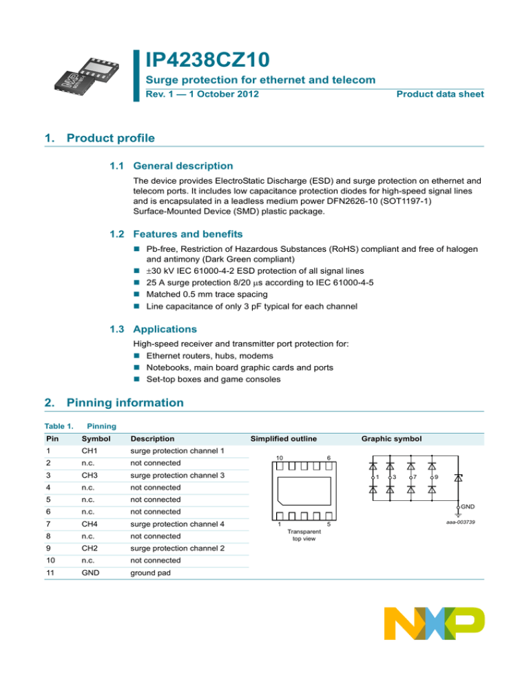
Table 1.
Pinning
Pin
Symbol
Description
1
CH1
surge protection channel 1
2
n.c.
not connected
3
CH3
surge protection channel 3
4
n.c.
not connected
5
n.c.
not connected
6
n.c.
not connected
7
CH4
surge protection channel 4
8
n.c.
not connected
9
CH2
surge protection channel 2
10
n.c.
not connected
11
GND
ground pad
Simplified outline
Graphic symbol
7UDQVSDUHQW
WRSYLHZ
DDD
IP4238CZ10
NXP Semiconductors
Surge protection for ethernet and telecom
3. Ordering information
Table 2.
Ordering information
Type number
IP4238CZ10
Package
Name
Description
Version
DFN2626-10
plastic thermal enhanced extremely thin small outline package;
no leads; 10 terminals; body 2.6 2.6 0.5 mm
SOT1197-1
4. Marking
Table 3.
Marking code
Type number
Marking code
IP4238CZ10
4238
5. Limiting values
Table 4.
Limiting values
In accordance with the Absolute Maximum Rating System (IEC 60134).
Symbol
Parameter
VI
input voltage
Conditions
Min
Max
Unit
0.5
+5.5
V
VESD
electrostatic discharge voltage
30
+30
kV
Tstg
storage temperature
55
+125
C
Tamb
ambient temperature
40
+125
C
[1]
[1]
IEC 61000-4-2; contact discharge
All pins to ground.
6. Characteristics
Table 5.
Characteristics
Tamb = 25 C unless otherwise specified.
Symbol
Parameter
Conditions
Min
Typ
Max
Unit
VBR
breakdown voltage
Itest = 1 mA
6
-
IRM
reverse leakage current
Vbias = 3 V
-
-
100
nA
VF
forward voltage
Itest = 1 mA
Cline
line capacitance
-
0.7
-
V
f = 1 MHz; Vbias = 2.5 V
[1]
-
3
-
pF
[1][2]
-
0.07
-
pF
-
0.23
-
Cline(mutual)
mutual line capacitance
f = 1 MHz; Vbias = 2.5 V
rdyn
dynamic resistance
surge
[3]
positive transient
-
0.23
-
IPP = 1 A
[3]
-
2.1
-
V
IPP = 10 A
[3]
-
4.0
-
V
IPP = 25 A
[3]
-
7.3
-
V
negative transient
VCL(ch)trt(pos)
[1]
positive transient channel
clamping voltage
V
This parameter is guaranteed by design.
[2]
Between signal pin and pin n.c.
[3]
According to IEC 61000-4-5 (8/20 s).
IP4238CZ10
Product data sheet
All information provided in this document is subject to legal disclaimers.
Rev. 1 — 1 October 2012
© NXP B.V. 2012. All rights reserved.
2 of 11
IP4238CZ10
NXP Semiconductors
Surge protection for ethernet and telecom
,
$
DDD
,
$
9&/9
tp = 100 ns; Transmission Line Pulse (TLP)
Fig 1.
DDD
9&/9
tp = 100 ns; Transmission Line Pulse (TLP)
Dynamic resistance with positive clamping
Fig 2.
Dynamic resistance with negative clamping
The device uses an advanced clamping structure showing a negative dynamic resistance.
This snap-back behavior strongly reduces the clamping voltage to the system behind the
ESD protection during an ESD event. Do not connect unlimited DC current sources to the
data lines to avoid keeping the ESD protection device in snap-back state after exceeding
breakdown voltage (due to an ESD pulse for instance).
DDD
9&/
9
9&/
9
DDD
,&/$
IEC 61000-4-5; tp = 8/20 s; positive pulse
(1) Tamb = 125 C
(2) Tamb = 75 C
(2) Tamb = 75 C
(3) Tamb = 25 C
(3) Tamb = 25 C
Dynamic resistance with positive clamping
IP4238CZ10
Product data sheet
,&/$
IEC 61000-4-5; tp = 8/20 s; negative pulse
(1) Tamb = 125 C
Fig 3.
Fig 4.
Dynamic resistance with negative clamping
All information provided in this document is subject to legal disclaimers.
Rev. 1 — 1 October 2012
© NXP B.V. 2012. All rights reserved.
3 of 11
IP4238CZ10
NXP Semiconductors
Surge protection for ethernet and telecom
DDD
,50
$
7DPE&
Vbias = 3 V
Fig 5.
Reverse leakage current as a function of ambient temperature; typical values
IP4238CZ10
Product data sheet
All information provided in this document is subject to legal disclaimers.
Rev. 1 — 1 October 2012
© NXP B.V. 2012. All rights reserved.
4 of 11
IP4238CZ10
NXP Semiconductors
Surge protection for ethernet and telecom
7. Application information
The device can be configured to protect line-to-line and line-to-ground configurations, as
well as parallel configurations to increase the clamping performance.
When designing the Printed-Circuit Board (PCB), consider the parasitic resistance of
traces for relatively long surge pulses. For signal integrity, give careful consideration to
basic high-speed routing guidelines, impedance matching, and signal coupling. Do not
connect the signal lines to unlimited current sources like for example, a battery.
QF
3+<
QF
5-
3+<
5-
QF
DDD
Fig 6.
Line-to-line surge protection of an ethernet
interface with IP4238CZ10
DDD
Fig 7.
Line-to-ground surge protection of an ethernet
interface with IP4238CZ10
QF
QF
3+<
5-
QF
QF
DDD
Fig 8.
Enhanced surge protection of an ethernet interface with IP4238CZ10 (ground pad floating)
IP4238CZ10
Product data sheet
All information provided in this document is subject to legal disclaimers.
Rev. 1 — 1 October 2012
© NXP B.V. 2012. All rights reserved.
5 of 11
IP4238CZ10
NXP Semiconductors
Surge protection for ethernet and telecom
8. Package outline
'LPHQVLRQVLQPP
Fig 9.
PLQ
PD[
PD[
Package outline DFN2626-10 (SOT1197-1)
9. Packing information
Table 6.
Packing methods
The indicated -xxx are the last three digits of the 12NC ordering code.[1]
Type number
Package
Description
Packing quantity
4000
IP4238CZ10
[1]
IP4238CZ10
Product data sheet
DFN2626-10 4 mm pitch, 8 mm tape and reel
(SOT1197-1)
-115
For further information and the availability of packing methods, see Section 13.
All information provided in this document is subject to legal disclaimers.
Rev. 1 — 1 October 2012
© NXP B.V. 2012. All rights reserved.
6 of 11
IP4238CZ10
NXP Semiconductors
Surge protection for ethernet and telecom
10. Soldering
Footprint information for reflow soldering of DFN2626-10 package
SOT1197-1
Hx
Gx
D
P
0.025
0.025
Ay
Gy
By
SPy
SLy
nSPy
Hy
nSPx
SPx
SLx
Generic footprint pattern
Refer to the package outline drawing for actual layout
solder land
solder paste deposit
solder land plus solder paste
occupied area
solder resist
DIMENSIONS in mm
P
Ay
By
D
SLx
SLy
SPx
SPy
Gx
Gy
Hx
Hy
0.5
3.05
1.9
0.25
2.2
1.3
0.8
0.4
2.5
2.85
2.85
3.3
Issue date
11-07-27
12-09-16
sot1197-1_fr
Fig 10. Reflow soldering footprint DFN2626-10 (SOT1197-1)
IP4238CZ10
Product data sheet
All information provided in this document is subject to legal disclaimers.
Rev. 1 — 1 October 2012
© NXP B.V. 2012. All rights reserved.
7 of 11
IP4238CZ10
NXP Semiconductors
Surge protection for ethernet and telecom
11. Revision history
Table 7.
Revision history
Document ID
Release date
Data sheet status
Change notice
Supersedes
IP4238CZ10 v.1
20121001
Product data sheet
-
-
IP4238CZ10
Product data sheet
All information provided in this document is subject to legal disclaimers.
Rev. 1 — 1 October 2012
© NXP B.V. 2012. All rights reserved.
8 of 11
IP4238CZ10
NXP Semiconductors
Surge protection for ethernet and telecom
12. Legal information
12.1 Data sheet status
Document status[1][2]
Product status[3]
Definition
Objective [short] data sheet
Development
This document contains data from the objective specification for product development.
Preliminary [short] data sheet
Qualification
This document contains data from the preliminary specification.
Product [short] data sheet
Production
This document contains the product specification.
[1]
Please consult the most recently issued document before initiating or completing a design.
[2]
The term ‘short data sheet’ is explained in section “Definitions”.
[3]
The product status of device(s) described in this document may have changed since this document was published and may differ in case of multiple devices. The latest product status
information is available on the Internet at URL http://www.nxp.com.
12.2 Definitions
Draft — The document is a draft version only. The content is still under
internal review and subject to formal approval, which may result in
modifications or additions. NXP Semiconductors does not give any
representations or warranties as to the accuracy or completeness of
information included herein and shall have no liability for the consequences of
use of such information.
Short data sheet — A short data sheet is an extract from a full data sheet
with the same product type number(s) and title. A short data sheet is intended
for quick reference only and should not be relied upon to contain detailed and
full information. For detailed and full information see the relevant full data
sheet, which is available on request via the local NXP Semiconductors sales
office. In case of any inconsistency or conflict with the short data sheet, the
full data sheet shall prevail.
Product specification — The information and data provided in a Product
data sheet shall define the specification of the product as agreed between
NXP Semiconductors and its customer, unless NXP Semiconductors and
customer have explicitly agreed otherwise in writing. In no event however,
shall an agreement be valid in which the NXP Semiconductors product is
deemed to offer functions and qualities beyond those described in the
Product data sheet.
12.3 Disclaimers
Limited warranty and liability — Information in this document is believed to
be accurate and reliable. However, NXP Semiconductors does not give any
representations or warranties, expressed or implied, as to the accuracy or
completeness of such information and shall have no liability for the
consequences of use of such information. NXP Semiconductors takes no
responsibility for the content in this document if provided by an information
source outside of NXP Semiconductors.
In no event shall NXP Semiconductors be liable for any indirect, incidental,
punitive, special or consequential damages (including - without limitation - lost
profits, lost savings, business interruption, costs related to the removal or
replacement of any products or rework charges) whether or not such
damages are based on tort (including negligence), warranty, breach of
contract or any other legal theory.
Notwithstanding any damages that customer might incur for any reason
whatsoever, NXP Semiconductors’ aggregate and cumulative liability towards
customer for the products described herein shall be limited in accordance
with the Terms and conditions of commercial sale of NXP Semiconductors.
Right to make changes — NXP Semiconductors reserves the right to make
changes to information published in this document, including without
limitation specifications and product descriptions, at any time and without
notice. This document supersedes and replaces all information supplied prior
to the publication hereof.
IP4238CZ10
Product data sheet
Suitability for use — NXP Semiconductors products are not designed,
authorized or warranted to be suitable for use in life support, life-critical or
safety-critical systems or equipment, nor in applications where failure or
malfunction of an NXP Semiconductors product can reasonably be expected
to result in personal injury, death or severe property or environmental
damage. NXP Semiconductors and its suppliers accept no liability for
inclusion and/or use of NXP Semiconductors products in such equipment or
applications and therefore such inclusion and/or use is at the customer’s own
risk.
Applications — Applications that are described herein for any of these
products are for illustrative purposes only. NXP Semiconductors makes no
representation or warranty that such applications will be suitable for the
specified use without further testing or modification.
Customers are responsible for the design and operation of their applications
and products using NXP Semiconductors products, and NXP Semiconductors
accepts no liability for any assistance with applications or customer product
design. It is customer’s sole responsibility to determine whether the NXP
Semiconductors product is suitable and fit for the customer’s applications and
products planned, as well as for the planned application and use of
customer’s third party customer(s). Customers should provide appropriate
design and operating safeguards to minimize the risks associated with their
applications and products.
NXP Semiconductors does not accept any liability related to any default,
damage, costs or problem which is based on any weakness or default in the
customer’s applications or products, or the application or use by customer’s
third party customer(s). Customer is responsible for doing all necessary
testing for the customer’s applications and products using NXP
Semiconductors products in order to avoid a default of the applications and
the products or of the application or use by customer’s third party
customer(s). NXP does not accept any liability in this respect.
Limiting values — Stress above one or more limiting values (as defined in
the Absolute Maximum Ratings System of IEC 60134) will cause permanent
damage to the device. Limiting values are stress ratings only and (proper)
operation of the device at these or any other conditions above those given in
the Recommended operating conditions section (if present) or the
Characteristics sections of this document is not warranted. Constant or
repeated exposure to limiting values will permanently and irreversibly affect
the quality and reliability of the device.
Terms and conditions of commercial sale — NXP Semiconductors
products are sold subject to the general terms and conditions of commercial
sale, as published at http://www.nxp.com/profile/terms, unless otherwise
agreed in a valid written individual agreement. In case an individual
agreement is concluded only the terms and conditions of the respective
agreement shall apply. NXP Semiconductors hereby expressly objects to
applying the customer’s general terms and conditions with regard to the
purchase of NXP Semiconductors products by customer.
No offer to sell or license — Nothing in this document may be interpreted or
construed as an offer to sell products that is open for acceptance or the grant,
conveyance or implication of any license under any copyrights, patents or
other industrial or intellectual property rights.
All information provided in this document is subject to legal disclaimers.
Rev. 1 — 1 October 2012
© NXP B.V. 2012. All rights reserved.
9 of 11
IP4238CZ10
NXP Semiconductors
Surge protection for ethernet and telecom
Export control — This document as well as the item(s) described herein
may be subject to export control regulations. Export might require a prior
authorization from competent authorities.
Quick reference data — The Quick reference data is an extract of the
product data given in the Limiting values and Characteristics sections of this
document, and as such is not complete, exhaustive or legally binding.
Non-automotive qualified products — Unless this data sheet expressly
states that this specific NXP Semiconductors product is automotive qualified,
the product is not suitable for automotive use. It is neither qualified nor tested
in accordance with automotive testing or application requirements. NXP
Semiconductors accepts no liability for inclusion and/or use of
non-automotive qualified products in automotive equipment or applications.
In the event that customer uses the product for design-in and use in
automotive applications to automotive specifications and standards, customer
(a) shall use the product without NXP Semiconductors’ warranty of the
product for such automotive applications, use and specifications, and (b)
whenever customer uses the product for automotive applications beyond
NXP Semiconductors’ specifications such use shall be solely at customer’s
own risk, and (c) customer fully indemnifies NXP Semiconductors for any
liability, damages or failed product claims resulting from customer design and
use of the product for automotive applications beyond NXP Semiconductors’
standard warranty and NXP Semiconductors’ product specifications.
12.4 Trademarks
Notice: All referenced brands, product names, service names and trademarks
are the property of their respective owners.
13. Contact information
For more information, please visit: http://www.nxp.com
For sales office addresses, please send an email to: salesaddresses@nxp.com
IP4238CZ10
Product data sheet
All information provided in this document is subject to legal disclaimers.
Rev. 1 — 1 October 2012
© NXP B.V. 2012. All rights reserved.
10 of 11
IP4238CZ10
NXP Semiconductors
Surge protection for ethernet and telecom
14. Contents
1
1.1
1.2
1.3
2
3
4
5
6
7
8
9
10
11
12
12.1
12.2
12.3
12.4
13
14
Product profile . . . . . . . . . . . . . . . . . . . . . . . . . . 1
General description . . . . . . . . . . . . . . . . . . . . . 1
Features and benefits . . . . . . . . . . . . . . . . . . . . 1
Applications . . . . . . . . . . . . . . . . . . . . . . . . . . . 1
Pinning information . . . . . . . . . . . . . . . . . . . . . . 1
Ordering information . . . . . . . . . . . . . . . . . . . . . 2
Marking . . . . . . . . . . . . . . . . . . . . . . . . . . . . . . . . 2
Limiting values. . . . . . . . . . . . . . . . . . . . . . . . . . 2
Characteristics . . . . . . . . . . . . . . . . . . . . . . . . . . 2
Application information. . . . . . . . . . . . . . . . . . . 5
Package outline . . . . . . . . . . . . . . . . . . . . . . . . . 6
Packing information . . . . . . . . . . . . . . . . . . . . . 6
Soldering . . . . . . . . . . . . . . . . . . . . . . . . . . . . . . 7
Revision history . . . . . . . . . . . . . . . . . . . . . . . . . 8
Legal information. . . . . . . . . . . . . . . . . . . . . . . . 9
Data sheet status . . . . . . . . . . . . . . . . . . . . . . . 9
Definitions . . . . . . . . . . . . . . . . . . . . . . . . . . . . . 9
Disclaimers . . . . . . . . . . . . . . . . . . . . . . . . . . . . 9
Trademarks. . . . . . . . . . . . . . . . . . . . . . . . . . . 10
Contact information. . . . . . . . . . . . . . . . . . . . . 10
Contents . . . . . . . . . . . . . . . . . . . . . . . . . . . . . . 11
Please be aware that important notices concerning this document and the product(s)
described herein, have been included in section ‘Legal information’.
© NXP B.V. 2012.
All rights reserved.
For more information, please visit: http://www.nxp.com
For sales office addresses, please send an email to: salesaddresses@nxp.com
Date of release: 1 October 2012
Document identifier: IP4238CZ10
