Evaluation Board for the
AD8333 I/Q Demodulator
AD8333-EVALZ
FEATURES
GENERAL DESCRIPTION
Factory tested and ready to use
SMA input and output connectors (7)
Configurable jumpers for user options
Phase select
Provision for external reset
Includes LNA input amplifier
Internal clock buffer
Summing amplifier to view sum of both channels or
single Channel I and Channel Q outputs
Compact surface-mount layout can be applied to
user application
The AD8333-EVAL evaluation board enables the user to quickly
become familiar with the operating characteristics and features
of the AD8333 dual I/Q demodulator and phase shifter. Jumpers
provide a convenient means for exercising the user-selectable
features of the AD8333.
The board is tested prior to shipment and shipped with the
phase-encoding bits set to 0000 (no phase shift) for both
channels. The LNA is set up for a 50 Ω source, and the VGA
sections of the AD8332 are disabled. Test points are provided
along the signal path to facilitate signal tracing.
APPLICATIONS
Hands-on testing of the AD8333
05836-001
EVALUATION BOARD
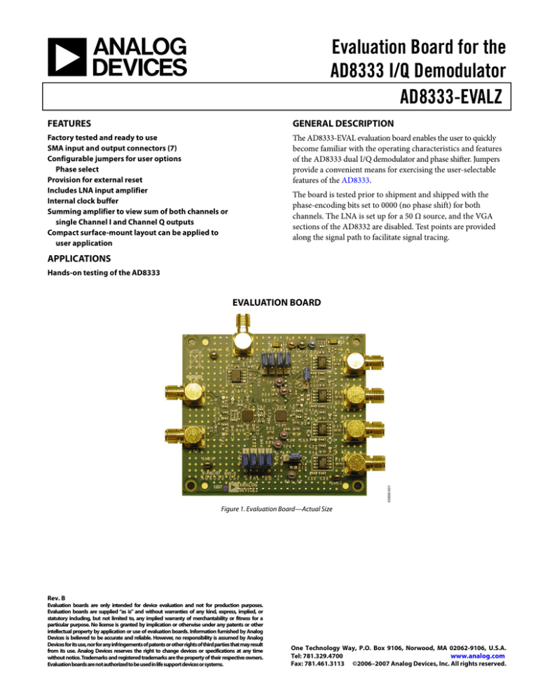
Figure 1. Evaluation Board—Actual Size
Rev. B
Evaluation boards are only intended for device evaluation and not for production purposes.
Evaluation boards are supplied “as is” and without warranties of any kind, express, implied, or
statutory including, but not limited to, any implied warranty of merchantability or fitness for a
particular purpose. No license is granted by implication or otherwise under any patents or other
intellectual property by application or use of evaluation boards. Information furnished by Analog
Devices is believed to be accurate and reliable. However, no responsibility is assumed by Analog
Devices for its use, nor for any infringements of patents or other rights of third parties that may result
from its use. Analog Devices reserves the right to change devices or specifications at any time
without notice. Trademarks and registered trademarks are the property of their respective owners.
Evaluation boards are not authorized to be used in life support devices or systems.
One Technology Way, P.O. Box 9106, Norwood, MA 02062-9106, U.S.A.
Tel: 781.329.4700
www.analog.com
Fax: 781.461.3113 ©2006–2007 Analog Devices, Inc. All rights reserved.
AD8333-EVALZ
TABLE OF CONTENTS
Features .............................................................................................. 1
Measurement Setup.......................................................................4
Applications....................................................................................... 1
Evaluation Board Schematic and Artwork.....................................5
General Description ......................................................................... 1
Board Layout..................................................................................7
Evaluation Board .............................................................................. 1
Ordering Information.......................................................................9
Revision History ............................................................................... 2
Bill of Materials..............................................................................9
Introduction ...................................................................................... 3
Ordering Guide .......................................................................... 10
Features and Options ................................................................... 3
ESD Caution................................................................................ 10
REVISION HISTORY
9/07—Rev. A to Rev. B
Changes to Features and Options Section..................................... 3
Changes to Figure 3.......................................................................... 5
Changes to Table 4............................................................................ 9
6/07—Rev. 0 to Rev. A
Changes to Figure 1.......................................................................... 1
Changes to Figure 2.......................................................................... 4
Changes to Figure 4.......................................................................... 6
Changes to Figure 6 and Figure 7................................................... 7
Changes to Table 4............................................................................ 9
Changes to Ordering Guide .......................................................... 10
1/06—Revision 0: Initial Version
Rev. B | Page 2 of 12
AD8333-EVALZ
INTRODUCTION
The AD8333-EVAL evaluation board provides a platform for
test and evaluation of the AD8333 I/Q demodulator and phase
shifter. The board is shipped fully assembled and tested, and the
user need only connect appropriate signals to the RF input and
f4LO SMA connectors. An AD8332 is included with the board
and acts as a buffer and bias supply for the AD8333, converting
single-ended signals to differential, centered at half the supply.
A photograph of the board is shown in Figure 1 and a schematic
diagram is shown in Figure 3. The board requires dual 5 V
supplies capable of supplying 300 mA or greater. Except for the
components shown in grayscale, the board is built and tested
using all the components illustrated in Figure 3.
FEATURES AND OPTIONS
The evaluation board has several features and options that are
configurable according to the specific needs of the user. Table 1
lists the jumpers and their functions.
Table 1. Jumper Functions
Jumper
ENBL
PH10
PH11
PH12
PH13
PH20
PH21
PH22
PH23
RST
Function
Enable the AD8333
Ch 1 Phase 0 bit
Ch 1 Phase 1 bit
Ch 1 Phase 2 bit
Ch 1 Phase 3 bit
Ch 2 Phase 0 bit
Ch 2 Phase 1 bit
Ch 2 Phase 2 bit
Ch 2 Phase 3 bit
Reset pin
Position
Bottom = disable; top = enable
Top = 0; bottom = 1
Top = 0; bottom = 1
Top = 0; bottom = 1
Top = 0; bottom = 1
Top = 1; bottom = 0
Top = 1; bottom = 0
Top = 1; bottom = 0
Top = 1; bottom = 0
Left = reset; right = normal
The Phase Bits
The phase bits configure the channel for one of sixteen 22.5°
increments from 0° to 337.5°. The increments increase according
to a simple binary code from 0000 to 1111 embodied in the
phase bits from 0° (0x0) to 337.5° (0xF). Table 2 lists the phase
shift and corresponding code for each bit. The bits labeled 0 and
1 correspond to low and high, respectively, on the silkscreen.
Jumpers are provided to select the desired state.
Enable and Reset Jumpers
Table 2. Phase Shift Select Codes
Ф Shift
0°
22.5°
45°
67.5°
90°
112.5°
135°
157.5°
180°
202.5°
225°
247.5°
270°
292.5°
315°
337.5°
PHx3
0
0
0
0
0
0
0
0
1
1
1
1
1
1
1
1
PHx2
0
0
0
0
1
1
1
1
0
0
0
0
1
1
1
1
PHx1
0
0
1
1
0
0
1
1
0
0
1
1
0
0
1
1
PHx0
0
1
0
1
0
1
0
1
0
1
0
1
0
1
0
1
Fixed Options
Several options can be realized by adding or changing resistors.
LNA Input Impedance
The shipping configuration of the input impedance of the LNA
is 50 Ω to match the output impedance of most signal generators.
Input impedances of up to 14.7 kΩ are obtained by selection of
the values of R9 and R10. Details concerning this circuit feature
are found in the AD8332 data sheet. For reference, Table 3 lists
common values of input impedance and corresponding
feedback resistor values.
Table 3. LNA External Component Values for Common
Source Impedances
RIN (Ω)
50
75
100
200
500
6k
For normal operation, place a jumper in the upper position of
ENBL. To disable the AD8333, move the jumper to the lower
position. For normal operation, the jumper for RST is in its
right position. When the jumper is in the left position, the
device counter is held in reset and no mixing occurs.
Rev. B | Page 3 of 12
RFB, Nearest STD 1% Value (Ω)
280
412
562
1.13 k
3.01 k
∞
CSH (pF)
22
12
8
1.2
None
None
AD8333-EVALZ
Current Summing
MEASUREMENT SETUP
The output transimpedance amplifiers, A1 through A4, are
configured as I-to-V converters to convert the output current of
the AD8333 to a voltage. The low-pass filters formed by the
feedback components are designed for single-channel operation
with ±5 V supplies.
Figure 2 displays the connector and user-selectable jumper
locations. A typical board and test equipment setup is shown in
Figure 4. Two signal generators, a power splitter, and a ±5 V,
300 mA (minimum) power supply are required. Synchronize
the signal generators for optimum results. Remember that the
f4LO signal generator frequency is four times that of the nominal
frequency of the RF source. For example, to detect signals with
a nominal center frequency of 5 MHz, an f4LO frequency of 20 MHz
is applied to the oscillator input. For an applied RF signal of
5.01 MHz, the mix frequencies are 10 kHz and 10.01 MHz.
Because of the low-pass active filter of the transconductance
amplifiers (A1 through A4), 10 kHz is observed at the output.
Optional R4 and R5 resistors are provided to sum the two
channels. When R4 and R5 are installed, R2 and R3 are
removed and the sum of the outputs is seen at the I1 and Q1
output SMA connectors. If large signal levels are expected, the
feedback resistor and capacitor values, 787 Ω and 2.2 nF, can be
halved and doubled, respectively, to optimize the output swing.
The filter capacitor values can be changed if other frequencies
are desired.
Reset Input
For normal operation, the reset input is high (no reset). To drive
the reset with a dynamic signal, provision is made to connect a
signal generator at the RST input. A 49.9 Ω, 0603 surfacemount resistor can be installed at R15 to terminate the reset
input for pulsed experiments. In this configuration, the jumper
at RST is not used and must be removed to avoid loading the
power supply.
Take care to avoid over driving the LNA input of the AD8332.
The LNA gain is 19 dB (9.5×) and the maximum output swing
must not be exceeded; −10 dBm suffices for many experiments.
The f4LO input is ac-coupled to a 5 V LVDS buffer to provide an
ideal interface to the AD8333.
The f4LO level is frequency dependent; consult the AD8333 data
sheet for minimum signal levels, then adjust the signal generator
output level accordingly.
f4LO INPUT
CHANNEL 1
PHASE BITS
+5V, GND, –5V
ENABLE
CH 1 I OUTPUT
CH 1 RF INPUT
CH 1 Q OUTPUT
CH 2 I OUTPUT
CH 2 RF INPUT
CHANNEL 2
PHASE BITS
Figure 2. Evaluation Board Layout
Rev. B | Page 4 of 12
RESET
05836-002
CH 2 Q OUTPUT
Rev. B | Page 5 of 12
Figure 3. Evaluation Board Schematic
IN2
L2
120nH
FB
IN1
L1
120nH
FB
VPS
R10
274Ω
VPS
C5
0.1µ F
C40
0.018µF
C3
22pF
TP1
C4
TP2 0.1µF
C6
0.1µF
C2
22pF
TP3
C1
TP4 0.1µF
8
7
6
5
4
3
2
1
LOP1
9
10
LOP2
LON2
VPS2
INH2
LMD2
LMD1
INH1
VPS1
LON1
31
COM1
COM2
32
30
VIP1
11
VIP2
C39
0.018µF
29
28
13
26
15
5
1
20
21
VOH2
6
7
0.1µF
R23
20Ω
R22
20Ω
R6
3.48kΩ
C13
0.1µF
17
18
3
LOP
4
R1
100Ω
C43
1nF
2
L5
120nH FB
+5V
R25
20Ω
C9
0. 1µF
Z3
DS90C401
22 VPS C42
VOL2 19
NC
VPSV
VOL1
COMM
16
24
VOH1 23
COMM
ENBV
25
RCLMP
VPS
+5V
C12
0.1µF
Z3 SPARE 8
C11
0.1µF
12
14
Z1
AD8332
27
HILO
MODE
R26
20Ω
R13
49.9Ω
R7
1.5kΩ
C17
0.1µF
8
7
6
5
4
3
2
1
10
PH23
PH22
PH21
L
PH20
9
PH21
PH22
PH23
LODC
4LON
4LOP
COMM
PH13
PH12
32 31
PH11
PH10
PH11
PH12
L PH13 H
PH10
PH20
C14
0.1µF
ENBL
GAIN
+
30
H
11
29
VPOS
+5V
VPOS
28
C7
10µF
10V
12
13
C8
10µF
10V
H
26
15
TP8
TP7
RST
17
18
19
20
R15
OPT
L
C51
0. 1µF
+5VS
+5VS
R2
0Ω
22 R4
OPT
21
23
24
H +5V
VPOS
RST
16
I2NO
I2PO
Q2PO
Q2NO
COMM
VNEG
Q1NO
Q1PO
I1PO
I1N0
25
ENBL
+5VS
C44
0. 1µF
7
–
+
4
+5VS
3
+5VS
7
–
+
4
7
–
3
+
4
7
–
3
+
4
C28
5pF
5
C52
0.1µF
C33
5pF
6
C32
2.2nF
–5V
–5V
R38
0Ω
I2
R35
Q2
0Ω
–5VS
–5VS
R42
787Ω
C30
5pF
6
R41
787Ω
C48
0.1µF
C31
2.2nF
A4
8 AD8021
1
2
5
5
–5VS
C47
0.1µF
L4
120nH FB
C50
0.1µF
A3
8 AD8021
1
2
C49
0.1µF
C36
0. 1µF
R5
OPT
+5VS
3
6
C29
2.2nF
R40
787Ω
–5VS
I1
R33
Q1
0Ω
R32
0Ω
L7
C27
5pF 120nH FB
6
C26
2.2nF
R39
787Ω
A2
8 AD8021
1
2
5
C45
0.1µF
A1
8 AD8021
1
2
C46
0.1µF
R3
0Ω
L6 +5VS
120nH FB
–5V
L3
120nH FB
TP5
C41
0.1µF
14
+
TP6
C24
0.1µF
27
DUT
AD8333
+5V
VPOS
R9
274Ω
VIN1
VIN2
RFIP
RF2P
VCM1
VCM2
RFIN
RF2N
–5V
ENBL
RSET
+5V
VPOS
VPOS
GND1 GND2 GND3 GND4
AD8333-EVALZ
EVALUATION BOARD SCHEMATIC AND ARTWORK
05836-003
AD8333-EVALZ
TOP:
SIGNAL GENERATOR FOR f4LO
INPUT TYPICAL SETTING: 20MHz
SIGNAL 1V p-p
BOTTOM:
GENERATOR FOR RF INPUT
TYPICAL SETTING: 5.01MHz
POWER
SUPPLY
SYNCHRONIZE
GENERATORS
+5V
–5V
POWER
SPLITTER
05836-004
SIGNAL
INPUT(S)
Figure 4. Typical Board Test Connections (One Channel Shown)
Rev. B | Page 6 of 12
AD8333-EVALZ
BOARD LAYOUT
05836-007
05836-005
The AD8333 evaluation board has four layers. The interconnecting circuitry is located on the outer layers with the inner layers dedicated
as power and ground planes. Figure 5 through Figure 9 illustrate the copper patterns.
Figure 7. Component Side Silkscreen
Figure 6. Wiring Side Copper
05836-008
05836-006
Figure 5. Component Side Copper
Figure 8. Ground Plane
Rev. B | Page 7 of 12
05836-009
AD8333-EVALZ
Figure 9. Power Plane
Rev. B | Page 8 of 12
AD8333-EVALZ
ORDERING INFORMATION
BILL OF MATERIALS
Table 4.
Qty
4
23
Name
IC
Capacitor
Description
AD8021ARZ
0.1 μF, 16 V, 0603, X7R
2
2
4
4
2
1
1
7
7
1
6
1
1
2
1
4
4
10
Capacitor
Capacitor
Capacitor
Capacitor
Capacitor
Capacitor
IC
Connector
Ferrite Bead
Resistor
Resistor
Resistor
Resistor
Resistor
Resistor
Resistor
Resistor
Header
22 pF, 50 V, 5%, 0603
10 μF, 10 V, A size tantalum
2.2 nF, 50 V, X7R, 10%, 0603
5 pF, 50 V, 0603
0.018 μF, 10%, 50 V, X7R, 0603
1 nF, 100 V, 10%, 0603, X7R
AD8333 I/Q demodulator
SMA female PC mount, RA
120 nH, 0603
100 Ω, 1%, 1/16 W, 0603
0 Ω, 5%, 1/10 W, 0603
3.48 kΩ, 1%, 1/10 W, 0603
1.5 kΩ, 1%, 1/10 W, 0603
274 Ω, 1/16 W, 1%, 0603
49.9 Ω, 1%, 1/16 W, 0603
20 Ω, 1%, 1/10 W, 0603
787 Ω, 1/16 W, 1%, 0603
3-pin 0.025" sq., 0.1" spacing
1
4
1
5
1
1
Test Loop
Test Loop
Test Loop
Test Loop
IC
IC
0.125” diameter, red
0.125” diameter, black
0.125” diameter, blue
0.125” diameter, purple
VGA AD8332
DRV LVDS dual differential
signal 8-lead SOIC
1
4
10
PC Board
Bumper
Jumper
Reference Designator
A1 to A4
C1, C4, C5, C6, C9, C11, C12, C13,
C14, C17, C24, C36, C41, C42,
C44, C45, C46, C47, C48, C49,
C50, C51, C52
C2, C3
C7, C8
C26, C29, C31, C32
C27, C28, C30, C33
C39, C40
C43
DUT
I1, I2, IN1, IN2, LOP, Q1, Q2
L1, L2, L3, L4, L5, L6, L7
R1
R2, R3, R32, R33, R35, R38
R6
R7
R9, R10
R13
R22, R23, R25, R26
R39 to R42
ENBL, PH10, PH11, PH12, PH13,
PH20, PH21, PH22, PH23, RST
+5 V
GND1 to GND4
−5 V
TP5 to TP8, RST
Z1
Z3
Mount to wiring side of board
Install at ENBL: top, PH10: top,
PH11: top, PH12: top, PH13: top,
PH20: bottom, PH21: bottom,
PH22: bottom, PH23: bottom,
RST: right; orient when board is in
normal viewing position with IN1
and IN2 SMA connectors at left
Rev. B | Page 9 of 12
Mfg. Part Number
AD8021ARZ
C0603C104K4RACTU
Manufacturer
Analog Devices, Inc.
KEMET Corporation
ECJ-1VC1H220J
T491A106M010AS
ECJ-1VB1H222K
ECJ-1VC1H050C
06035C183KAT2A
ECJ-1VB2A102K
AD8333ACPZ-WP
901-143-6RFX
BLM18BA750SN1D
ERJ-3EKF1000V
ERJ-2GE0R00X
ERJ-3EKF3.48KV
ERJ3EKF1501V
ERJ-3EKF2740V
ERJ-3EKF49R9V
ERJ3EKF20R0V
ERJ-3EKF7870V
22-11-2032
Panasonic
KEMET Corporation
Panasonic
Panasonic
AVX Corp.
Panasonic
Analog Devices, Inc.
Amphenol
Murata Manufacturing Co.
Panasonic
Panasonic
Panasonic
Panasonic
Panasonic
Panasonic
Panasonic
Panasonic
Molex, Inc.
TP-104-01-02
TP-104-01-00
TP-104-01-06P
TP-104-01-07
AD8332ACPZ
DS90C401M
Components Corp.
Components Corp.
Components Corp.
Components Corp.
Analog Devices, Inc.
National Semiconductor
09-A00941C
SJ-67A11 (black)
65474-001
3M
FCI
AD8333-EVALZ
ORDERING GUIDE
Model
AD8333-EVALZ 1
1
ESD CAUTION
Description
Evaluation Board
Z = RoHS Compliant Part.
Rev. B | Page 10 of 12
AD8333-EVALZ
NOTES
Rev. B | Page 11 of 12
AD8333-EVALZ
NOTES
©2006–2007 Analog Devices, Inc. All rights reserved. Trademarks and
registered trademarks are the property of their respective owners.
EB05836-0-9/07(B)
Rev. B | Page 12 of 12
