SC632A
1MHz Fixed 5.0V Output
Charge Pump Regulator
POWER MANAGEMENT
Features
Description
Input voltage range — 2.95V to 5.5V
VOUT tolerance — 5.0V ±3%
Continuous output current — 275mA
Peak output current — 400mA
Three charge pump modes — 1x, 1.5x and 2x
Output ripple voltage — 50mVPP , typical
Short circuit, over-voltage, and over-temperature
protection
Soft-start functionality
Shutdown current — 0.1µA, typical
Ultra thin package — 2 x 2 x 0.6 (mm)
Lead-free and halogen-free
WEEE and RoHS compliant
Applications
Mobile phones
Tablets
USB On-The-Go
Multi-LED backlit LCDs
Compact flash/CF+ products
Digital video cameras
DVI/HDMI ports
Wi-Fi base stations
Modems
Set-top boxes
The SC632A is a high-current voltage regulator using
Semtech’s proprietary low-noise charge pump technology. The charge pump provides a low EMI solution
compared to inductive boost regulators. Performance is
optimized for use in single Li-Ion battery cell applications.
The regulator provides the performance of a linear, low
drop-out (LDO) voltage regulator when the input is greater
than 5.0V. Unlike an LDO, drop-out is avoided when the
input is less than 5.0V. Instead, a charge pump is activated
to provide voltage boost and the head-room needed for
voltage regulation.
The SC632A’s charge pump has three modes of operation:
2x, 1.5x, and 1x modes. 2x and 1.5x are voltage boost
modes that deliver current to the load in each of two
phases. The 1x mode turns off the charge pump, delivering current through an LDO. Hysteresis is provided to
prevent chatter between charge pump modes. When
active, the charge pump provides low-ripple operation at
1MHz. Typically the output ripple is 50mVpp at the
maximum continuous current rating of 275mA.
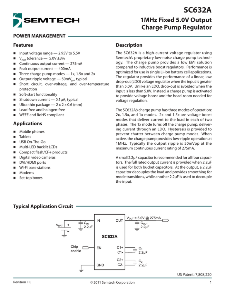
A small 2.2µF capacitor is recommended for all four capacitors. The full rated output current is provided when 2.2µF
is used for both bucket capacitors. At the output, a 2.2µF
capacitor decouples the load and provides smoothing for
mode transitions, while another 2.2µF is used to decouple
the input.
Typical Application Circuit
CIN
2.2µF
VBAT
IN
OUT
VOUT = 5.0V @ 275mA
COUT
2.2µF
SC632A
Chip
enable
EN
GND
C1+
C1-
C1
2.2µF
C2+
C2-
C2
2.2µF
US Patent: 7,808,220
Revision 1.0
© 2011 Semtech Corporation
SC632A
Pin Configuration
GND
Ordering Information
1
8
C2-
TOP VIEW
C1+
2
7
C2+
C1-
3
6
OUT
5
EN
Device
Package
SC632AULTRT(1)(2)
MLPD-UT-8 2x2
SC632AEVB
Evaluation Board
Notes:
(1) Available in tape and reel only. A reel contains 3,000 devices.
(2) Lead-free packaging only. Device is WEEE and RoHS compliant,
and halogen-free.
T
IN
4
MLPD-UT-8; 2x2, 8 LEAD
θJA = 68°C/W
Marking Information
K2A
yw
Yw = Datecode
SC632A
Absolute Maximum Ratings
Recommended Operating Conditions
IN (V) . . . . . . . . . . . . . . . . . . . . . . . . . . . . . . . . . . . -0.3 to +6.0
Ambient Temperature Range (°C). . . . . . . . . -40 ≤ TA ≤ +85
OUT (V). . . . . . . . . . . . . . . . . . . . . . . . . . . . . . . . . -0.3 to +6.0
IN (V)..... . . . . . . . . . . . . . . . . . . . . . . . . . . . . . . . . . 2.95 ≤ VIN ≤ 5.5
C1+, C2+ (V) . . . . . . . . . . . . . . . . . . . . . . . . . -0.3 to (VOUT + 0.3)
Pin Voltage — All Other Pins (V). . . . . . . . . -0.3 to (VIN + 0.3)
OUT pin — Short Circuit Duration . . . . . . . . . . . Continuous
ESD Protection Level(2) (kV) . . . . . . . . . . . . . . . . . . . . . . . . . . . . 4
Thermal Information
Thermal Resistance, Junction to Ambient(1) (°C/W) . . . . 68
Maximum Junction Temperature (°C). . . . . . . . . . . . . . . +150
Storage Temperature Range (°C). . . . . . . . . . . . . -65 to +150
Peak IR Reflow Temperature (10s to 30s) (°C) . . . . . . . . +260
Exceeding the above specifications may result in permanent damage to the device or device malfunction. Operation outside of the parameters
specified in the Electrical Characteristics section is not recommended.
NOTES
(1) Calculated from package in still air, mounted to 3 x 4.5 (in), 4 layer FR4 PCB with thermal vias under the exposed pad per JESD51 standards.
(2) Tested according to JEDEC standard JESD22-A114-B.
Electrical Characteristics
Unless otherwise specified: TA = +25°C for Typ, -40°C to +85°C for Min and Max; CIN = COUT = C1 = C2 = 2.2µF (ESR < 0.03Ω); VIN = 2.95V to 5.5V
Parameter
Symbol
Condition
Min
Typ
Max
Units
Output Voltage
VOUT
VIN = 4.2V, IOUT = 1mA
4.85
5.0
5.15
V
Output Voltage Ripple
VPP
IOUT = 275mA
Maximum Output Current
IOUT
50
mV
Peak Load - thermally limited(1),
TJ <150°C, 3.4V ≤ VIN ≤ 5.5V
400
mA
Continuous Load,
3.10V ≤ VIN ≤ 4.2V
275
mA
Shutdown Current
ISD
Shutdown (EN = GND), VIN = 3.6V
0.1
2
µA
Total Quiescent Current
IQ
EN high, IOUT = 1mA
2.5
3.5
mA
Charge Pump Frequency
fPUMP
VIN = 3.2V
1
MHz
tSU
(EN transitions from low to high),
4.85V ≤ VOUT ≤ 5.15V, No load
400
µs
Line Regulation
ΔVLINE
IOUT = 1mA, 2.95V ≤ VIN ≤ 4.2V
21
mV
Load Regulation
ΔVLOAD
VIN =4.2V, 1mA ≤ IOUT ≤ 400mA
37.5
mV
Start-Up Time
SC632A
Electrical Characteristics (continued)
Parameter
Symbol
Condition
Min
EN Input High Threshold
VIH
VIN = 5.5V
1.6
EN Input Low Threshold
VIL
VIN = 2.95V
0.4
V
EN Input High Current
IIH
VIN = 5.5V
2
µA
EN Input Low Current
IIL
VIN = 5.5V
2
µA
Open-Loop Output Resistance
Mode Transition Voltage (2)
Typ
Max
Units
V
1x mode
0.25
Ω
1.5x mode, VIN = 3.7V
3.5
Ω
2x mode, VIN = 3.1V
4.5
Ω
V TRANS 1X
IOUT = 200mA
5.05
V
V TRANS 1.5X
IOUT = 200mA
3.8
V
ISC
VOUT = 0V, IOUT = IIN
300
600
980
mA
VOUT > 2V, 1x mode
0.6
1.2
2.0
A
VOUT > 2V, 1.5x and 2x modes
1.2
2.0
2.8
A
ROUT
Fault Protection
Short-Circuit Current
Input Current Limit
Over Temperature
ILIMIT
VOUT ≤ 2V, IOUT = IIN
700
mA
TOTP
Rising Threshold
165
°C
THYS
Hysteresis(3)
20
°C
Notes:
(1) Thermal limitation is dependent upon the thermal performance of the printed circuit board in support of the package standard of 68° C/W.
(2) Voltage at the IN pin where a mode transition takes place in the charge pump with VIN falling.
(3) Guaranteed by design — not tested in production.
SC632A
Typical Characteristics
Line Regulation
Load Regulation
VOUT= 5.0V, VIN = 4.2V
25
20
Output Voltage Variation — ΔV LINE (mV)
Output Voltage Variation — ΔVLOAD (mV)
25
TA=25°C
15
TA=-40°C
TA=85°C
10
5
VOUT= 5.0V, IOUT = 1mA
20
85°C
15
25°C
10
3.6V, 0mV
-40°C
5
0
-5
-10
0
0
80
160
240
Output Current (mA)
320
-15
2.7
400
3.1
3.5
3.9
4.3
Input Voltage (V)
PSRR versus Frequency — 1x Mode
0
4.7
5.1
5.5
Output Ripple
VIN = 5.25V, VOUT= 5V, IOUT = 50mA; CIN = COUT = C1 = C2 = 2.2uF (0603)
120
VOUT= 5V; CIN = COUT = C1 = C2 = 2.2uF (0603)
-10
-20
100
400mA
80
300mA
Ripple (mV p-p)
Gain (dB)
-30
-40
-50
-60
-70
1.5x and 2x mode
60
200mA
40
100mA
50mA
-80
20
-90
-100
10
100
Frequency (Hz)
1000
0
10000
5.6
0
-10
-10
-20
-20
-30
-30
-40
-40
Gain (dB)
Gain (dB)
VIN = 4.2V, VOUT= 5V, IOUT = 50mA; CIN = COUT = C1 = C2 = 2.2uF (0603)
-50
-60
-80
-80
-90
-90
-100
-100
Frequency (Hz)
1000
4.0
4.4
Input Voltage (V)
3.6
3.2
2.8
10000
VIN = 2.9V, VOUT= 5V, IOUT = 50mA; CIN = COUT = C1 = C2 = 2.2uF (0603)
-60
-70
100
4.8
-50
-70
10
5.2
PSRR versus Frequency — 2x Mode
PSRR versus Frequency — 1.5x Mode
0
10mA
1x mode
10
100
Frequency (Hz)
1000
10000
SC632A
Typical Characteristics (continued)
Efficiency — 50mA
Efficiency — 10mA
90
1x Mode
Efficiency(%)
80
2x Mode
70 1x Mode
Mode
Transition
Hysteresis
1.5x Mode
60
2x Mode
1.5x Mode
50
2x Mode
1x Mode
70
60
5.6
5.2
4.8
4.4
4.0
Input Voltage (V)
3.6
3.2
30
5.6
2.8
5.2
1x Mode
2x Mode
1.5x Mode
Efficiency(%)
Efficiency(%)
70
2x Mode
40
5.2
4.8
4.4
4.0
Input Voltage (V)
3.6
3.2
2.8
30
5.6
5.2
4.8
4.4
4.0
Input Voltage (V)
3.6
100
3.2
2.8
VOUT= 5.0V, IOUT = 400mA, TA = 25°C
1x Mode
Mode
Transition
Hysteresis
90
1.5x Mode
80
Efficiency(%)
2x Mode
Mode
Transition
Hysteresis
1.5x Mode
2x Mode
50
2x Mode
70
60
Mode Transition
Hysteresis
1x
Mode
50
2x Mode
1.5x Mode
40
40
30
5.6
2.8
1.5x Mode
1.5x Mode
70
60
3.2
Mode
Transition
Hysteresis
Efficiency — 400mA
Mode
Transition
Hysteresis
1x
Mode
2.8
2x Mode
1.5x Mode
Efficiency — 300mA
VOUT= 5.0V, IOUT = 300mA, TA = 25°C
1x Mode
3.2
2x Mode
40
5.6
1x Mode
60
50
Efficiency(%)
3.6
4.4
4.0
Input Voltage (V)
70
50
80
4.8
Mode
Transition
Hysteresis
80
Mode
Transition
Hysteresis
1.5x Mode
60
1x Mode
90
1x Mode
80
90
2x Mode
VOUT= 5.0V, IOUT = 200mA, TA = 25°C
100
Mode
Transition
Hysteresis
90
100
1.5x Mode
Efficiency — 200mA
Efficiency — 100mA
30
Mode
Transition
Hysteresis
1.5x Mode
40
VOUT= 5.0V, IOUT = 100mA, TA = 25°C
100
Mode
Transition
Hysteresis
50
40
30
1x Mode
90
Mode
Transition
Hysteresis
80
VOUT= 5.0V, IOUT = 50mA, TA = 25°C
100
Efficiency(%)
100
VOUT= 5.0V, IOUT = 10mA, TA = 25°C
5.2
4.8
4.4
4.0
Input Voltage (V)
3.6
3.2
2.8
30
5.6
5.2
4.8
4.4
4.0
Input Voltage (V)
3.6
SC632A
Typical Characteristics (continued)
Ripple — 1x Mode
Ripple — 1.5x Mode
VIN = 5.2V, VOUT = 5.0V, IOUT = 275mA; CIN = COUT = C1 = C2 = 2.2uF (0603)
VIN = 4.2V, VOUT= 5.0V, IOUT = 275mA; CIN = COUT = C1 = C2 = 2.2uF (0603)
VIN -PP (100mV/div)
VIN -PP (100mV/div)
VOUT -PP (100mV/div)
VOUT -PP (100mV/div)
IOUT (200mA/div)
275mA
275mA
IOUT (200mA/div)
0mA
0mA
Time (400ns/div)
Time (400ns/div)
Startup (No Load)
Ripple — 2x Mode
VIN = 3.2V, VOUT = 5.0V, IOUT = 275mA; CIN = COUT = C1 = C2 = 2.2uF (0603)
VEN (2V/div)–
VIN -PP (100mV/div)
0V—
VOUT -PP (100mV/div)
IOUT (200mA/div)
VIN = 3.6V, IOUT = 0mA; CIN = COUT = C1 = C2 = 2.2uF (0603)
VOUT (2V/div)–
0V—
275mA
0V—
0mA
IOUT (200mA/div)
Time (200µs/div)
Time (400ns/div)
Quiescent Current
Startup (400mA)
VIN = 3.6V, IOUT = 400mA; CIN = COUT = C1 = C2 = 2.2uF (0603)
4
VOUT = 5V, IOUT = 1mA
3.5
VEN (2V/div)–
0V —
2x Mode
1.5x Mode
IQ(mA)
3
VOUT (2V/div)–
0V—
2x Mode
2.5
1x Mode
1.5x Mode
2
1x Mode
0V—
IOUT (200mA/div)–
1.5
Time (200µs/div)
1
5.6
5.2
4.8
4.4
4.0
Input Voltage (V)
3.6
3.2
2.8
SC632A
Pin Descriptions
Pin
Pin Name
Pin Function
1
GND
Ground — connect to ground plane with multiple vias
2
C1+
Positive terminal of bucket capacitor 1
3
C1-
Negative terminal of bucket capacitor 1
4
IN
Input supply voltage
5
EN
Chip enable — active-high
6
OUT
Output
7
C2+
Positive terminal of bucket capacitor 2
8
C2-
Negative terminal of bucket capacitor 2
T
Thermal Pad
This pad is for heat sinking and is not connected internally. It must be connected to a ground plane using
multiple vias.
SC632A
Block Diagram
IN 4
LDO
2 C1+
1MHz
3 C17 C2+
EN 5
Logic
Control
Reference
Voltage
Generator
CHARGE
PUMP
8 C26 OUT
1 GND
SC632A
Applications Information
General Description
Temperature Derating
The SC632A is a 5.0V output charge pump regulator
designed to support up to 300mA (TA ≤ 80°C, 3.15V ≤ VIN ≤
4.2V) and 275mA (TA ≤ 85°C, 3.15V ≤ VIN ≤ 5.5V) of continuous current for powering 5.0V devices in portable
handheld equipment including Compact Flash and CF+
products.
The VIN supply range and ambient temperature range of
the application should be compared with the following
derating curve to determine the maximum safe continuous load current. The DC operating points beneath each
curve are in the safe operating temperature range of the
MLP package.
450
400
300
Derating for VIN < 5.5V
250
200
150
Thermal Resistance
The SC632A package is thermally efficient when the circuit
board layout connects the thermal pad through multiple
vias to the ground plane. The thermal resistance rating is
dependent upon the connection between the thermal
pad and the ground plane. A layout that is done correctly
should keep the junction temperature below the overtemperature limit while operating the SC632A within the
specified electrical conditions. A poor layout may allow
the junction temperature to reach the over temperature
limit, so it is important to maintain adequate ground plane
around the device to maximize heat transfer to the PCB.
35
45
55
75
65
Ambient Temp (°C)
85
95
105
Maximum Continuous Output
Mode Transition Hysteresis
Hysteresis is provided to prevent chatter between charge
pump modes for input steps of up to 120mV. Decouple
the input to prevent steps greater than 120mV, for
optimum transient performance, when the input voltage
reaches the mode transition thresholds.
Derating for VIN < 4.2V
350
IOUT (mA)
The SC632A has three operating modes — 1x, 1.5x, and
2x. The 1x mode is a linear series regulation mode with a
low open-loop output resistance of only 250mW. The 1x
mode functions as a low-noise series linear regulator. The
1.5x and 2x modes are a low noise, constant frequency,
constant duty cycle switch mode, using two bucket
capacitors. One bucket supports the full output current
while the other bucket charges from the input. The two
buckets exchange roles in the next phase, supplying continuous output current in both phases and reducing the
need for a large output decoupling capacitor. The constant
frequency, constant duty cycle operation also produces
predictable constant frequency harmonics.
Protection Circuitry
The SC632A also provides protection circuitry that prevents the device from operating in an unspecified state.
These functions include:
•
•
•
Over-Current Protection (OCP)
Short-Circuit Current Protection (SCCP)
Over-Temperature Protection (OTP)
Over-Current Protection
Over-current protection is provided to limit the output
current. When VOUT is greater than 2V, OCP limits the
output to 1A typical. The threshold at 2V allows the
device to recover from excessive voltage droop during an
over current.
10
SC632A
Applications Information (continued)
Short-Circuit Current Protection
Short-circuit current protection is provided to limit the
current that can be sourced when the output is shorted to
ground. When a short circuit forces VOUT to drop below 2V,
the SCCP detects the condition and limits the output
current to 600mA (typical).
Over-Temperature Protection
The over-temperature circuit helps prevent the device
from overheating and experiencing a catastrophic failure.
When the junction temperature exceeds 165°C, the device
is disabled. It remains disabled until the junction temperature drops below this threshold. Hysteresis is included
that prevents the device from re-enabling until the junction temperature is reduced by 20°C.
Table 1 — Recommended Capacitors
Size Code
mil(mm)
Value
μF
CIN , COUT
0603(1608)
2.2
C1, C2
CIN , COUT
0402(1005)
2.2
C1, C2
Capacitor Selection
The SC632A is designed to use low-ESR ceramic capacitors
for the input and output bypass capacitors as well as the
charge pump bucket capacitors. The value of input, output
and decoupling capacitors will vary with system requirements for ripple and output current. Performance as
shown in the Typical Characteristic section is expected
when using 2.2µF capacitors in the 0603(1608 metric) case
size with X5R dieletric for CIN , COUT , C1 and C2 capacitors
(refer to Table 1).
Consider the DC voltage characteristic of the capacitor
when choosing capacitors for an application. The value of
capacitance at the DC operating voltage may be considerably lower than the rated value. The following table lists
recommended capacitor values which have been chosen
to minimize the impact of this limitation.
Capacitor
CIN , COUT
0402(1005)
0.47
C1, C2
1.0
CIN , COUT
0402(1005)
0.1
C1, C2
Notes
This capacitor is required for
the full rated output current.
Typical output VPP < 100mV
in all charge pump modes.
This capacitor combination supports up to 200mA
output current with typical
output VPP < 100mV in all
charge pump modes.
This capacitor combination supports up to 100mA
output current with typical
output VPP < 100mV in all
charge pump modes.
This combination of capacitors support up to 100mA
output current with typical
output VPP < 100mV in all
charge pump modes.
The 0.1µF bucket capacitors will increase output
resistance by 2.5Ω compared
to 0.47µF and larger values.
So, at 100mA output the 1.5x
to 2x mode transition will be
200mV higher.
NOTE: Use only X5R type capacitors, with a 6.3V rating or higher
The highest capacitance values in the smallest package
sizes tend to have poor DC voltage characteristics. The
highest value 0402 size capacitor retains as little as 35% of
its rated value at 5VDC. The same value chosen in the next
larger package size, 0603, will retain about 60% of its rated
value at 5VDC.
11
SC632A
Applications Information (continued)
PCB Layout Considerations
Poor layout can degrade the performance of the regulator and can be a contributory factor in EMI problems,
ground bounce, thermal issues, and resistive voltage
losses. Poor regulation and instability can result.
The following design rules are recommended:
. Place the bucket capacitors as close to the device as
possible and on the same side of the board. Use short
wide copper areas between the capacitor pins and
the device pins.
2. Place the input and output decoupling capacitors
as close as possible to the device and connect these
capacitors’ ground pads together to the ground plane
using multiple vias through a short wide copper
area.
3. Connect pin 1 directly to the copper area under the
thermal pad.
4. The thermal pad at the center of the device is not
electrically connected. Connect this pad to the
ground plane using multiple vias.
5. Use a ground plane to further reduce noise
interference on sensitive circuit nodes.
SC632A
C2-
GND
C1
C1+
GND
C2
C2+
C1-
OUT
IN
EN
COUT
CIN
EN
12
SC632A
Outline Drawing — MLPD-UT-8 2x2
B
D
A
DIMENSIONS
DIM
E
PIN 1
INDICATOR
(LASER MARK)
A
SEATING
PLANE
aaa C
A2
A1
C
A
A1
A2
b
D
D1
E
E1
e
L
N
aaa
bbb
INCHES
MIN
.020
.000
NOM
(.006)
MILLIMETERS
MAX
.024
.002
.007
.075
.061
.075
.026
.010 .012
.079 .083
.067 .071
.079 .083
.031 .035
.020 BSC
.012
.014 .016
8
.003
.004
MIN
0.50
0.00
NOM
-
(0.1524)
0.18 0.25
1.90 2.00
1.55 1.70
1.90 2.00
0.65 0.80
0.50 BSC
0.30 0.35
8
0.08
0.10
MAX
0.60
0.05
0.30
2.10
1.80
2.10
0.90
0.40
D1
1
E/2
2
LxN
E1
N
bxN
bbb
e
C A B
e/2
D/2
NOTES:
1.
CONTROLLING DIMENSIONS ARE IN MILLIMETERS (ANGLES IN DEGREES).
2.
COPLANARITY APPLIES TO THE EXPOSED PAD AS WELL AS THE TERMINALS.
13
SC632A
Land Pattern — MLPD-UT-8 2x2
H
R
(C)
DIMENSIONS
K
G
Z
Y
P
DIM
INCHES
MILLIMETERS
C
(.077)
(1.95)
G
.047
1.20
H
.067
1.70
K
.031
0.80
P
.020
0.50
R
.006
0.15
X
.012
0.30
Y
.030
0.75
Z
.106
2.70
X
NOTES:
1.
CONTROLLING DIMENSIONS ARE IN MILLIMETERS (ANGLES IN DEGREES).
2.
THIS LAND PATTERN IS FOR REFERENCE PURPOSES ONLY.
CONSULT YOUR MANUFACTURING GROUP TO ENSURE YOUR
COMPANY'S MANUFACTURING GUIDELINES ARE MET.
3.
THERMAL VIAS IN THE LAND PATTERN OF THE EXPOSED PAD
SHALL BE CONNECTED TO A SYSTEM GROUND PLANE.
FAILURE TO DO SO MAY COMPROMISE THE THERMAL AND/OR
FUNCTIONAL PERFORMANCE OF THE DEVICE.
14
SC632A
© Semtech 2011
All rights reserved. Reproduction in whole or in part is prohibited without the prior written consent of the copyright
owner. The information presented in this document does not form part of any quotation or contract, is believed to be
accurate and reliable and may be changed without notice. No liability will be accepted by the publisher for any consequence of its use. Publication thereof does not convey nor imply any license under patent or other industrial or
intellectual property rights. Semtech assumes no responsibility or liability whatsoever for any failure or unexpected
operation resulting from misuse, neglect improper installation, repair or improper handling or unusual physical or electrical stress including, but not limited to, exposure to parameters beyond the specified maximum ratings or operation
outside the specified range.
SEMTECH PRODUCTS ARE NOT DESIGNED, INTENDED, AUTHORIZED OR WARRANTED TO BE SUITABLE FOR USE IN LIFESUPPORT APPLICATIONS, DEVICES OR SYSTEMS OR OTHER CRITICAL APPLICATIONS. INCLUSION OF SEMTECH PRODUCTS
IN SUCH APPLICATIONS IS UNDERSTOOD TO BE UNDERTAKEN SOLELY AT THE CUSTOMER’S OWN RISK. Should a customer
purchase or use Semtech products for any such unauthorized application, the customer shall indemnify and hold
Semtech and its officers, employees, subsidiaries, affiliates, and distributors harmless against all claims, costs damages
and attorney fees which could arise.
Notice: All referenced brands, product names, service names and trademarks are the property of their respective
owners.
Contact Information
Semtech Corporation
Power Management Products Division
200 Flynn Road, Camarillo, CA 93012
Phone: (805) 498-2111 Fax: (805) 498-3804
www.semtech.com
15


