10 W, Failsafe, GaAs, SPDT Switch
0.2 GHz to 2.7 GHz
HMC546LP2E
Data Sheet
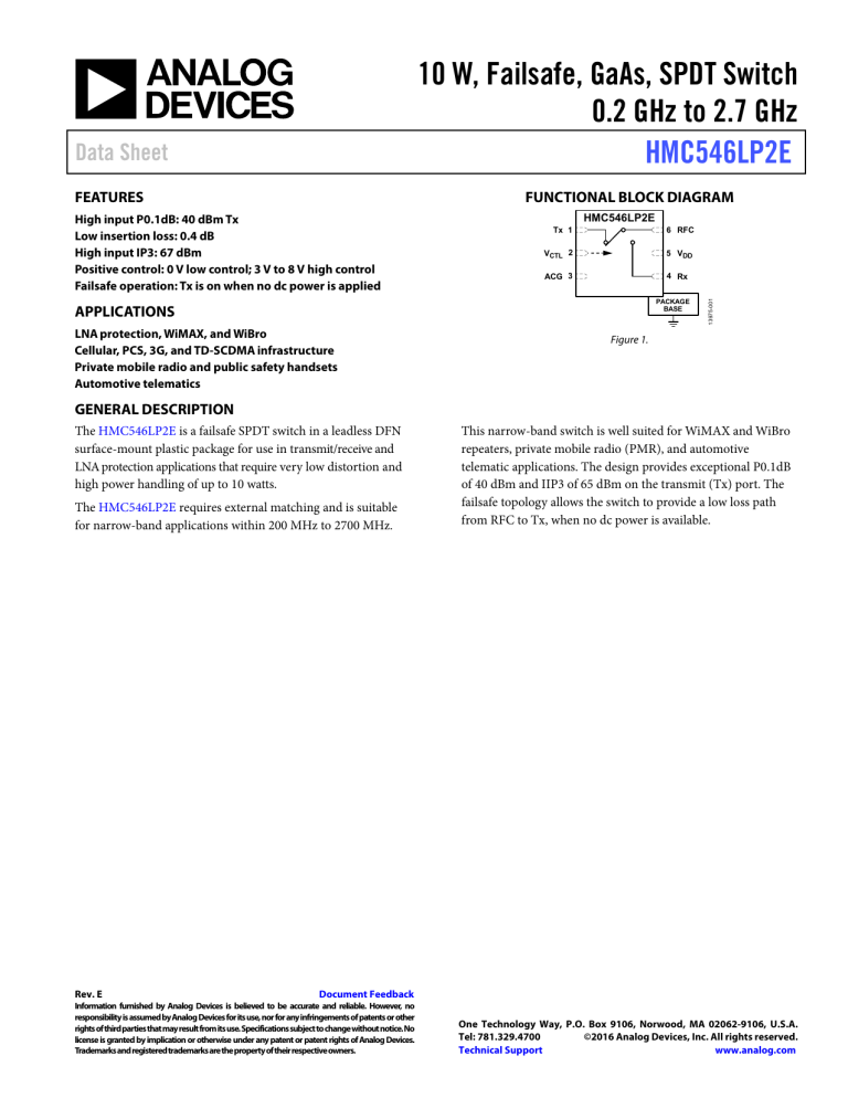
FUNCTIONAL BLOCK DIAGRAM
High input P0.1dB: 40 dBm Tx
Low insertion loss: 0.4 dB
High input IP3: 67 dBm
Positive control: 0 V low control; 3 V to 8 V high control
Failsafe operation: Tx is on when no dc power is applied
HMC546LP2E
Tx 1
6 RFC
VCTL 2
5 VDD
ACG 3
4 Rx
PACKAGE
BASE
APPLICATIONS
LNA protection, WiMAX, and WiBro
Cellular, PCS, 3G, and TD-SCDMA infrastructure
Private mobile radio and public safety handsets
Automotive telematics
13975-001
FEATURES
Figure 1.
GENERAL DESCRIPTION
The HMC546LP2E is a failsafe SPDT switch in a leadless DFN
surface-mount plastic package for use in transmit/receive and
LNA protection applications that require very low distortion and
high power handling of up to 10 watts.
The HMC546LP2E requires external matching and is suitable
for narrow-band applications within 200 MHz to 2700 MHz.
Rev. E
This narrow-band switch is well suited for WiMAX and WiBro
repeaters, private mobile radio (PMR), and automotive
telematic applications. The design provides exceptional P0.1dB
of 40 dBm and IIP3 of 65 dBm on the transmit (Tx) port. The
failsafe topology allows the switch to provide a low loss path
from RFC to Tx, when no dc power is available.
Document Feedback
Information furnished by Analog Devices is believed to be accurate and reliable. However, no
responsibility is assumed by Analog Devices for its use, nor for any infringements of patents or other
rights of third parties that may result from its use. Specifications subject to change without notice. No
license is granted by implication or otherwise under any patent or patent rights of Analog Devices.
Trademarks and registered trademarks are the property of their respective owners.
One Technology Way, P.O. Box 9106, Norwood, MA 02062-9106, U.S.A.
Tel: 781.329.4700
©2016 Analog Devices, Inc. All rights reserved.
Technical Support
www.analog.com
HMC546LP2E* Product Page Quick Links
Last Content Update: 08/30/2016
Comparable Parts
Design Resources
View a parametric search of comparable parts
•
•
•
•
Evaluation Kits
• HMC546LP2 Evaluation Board.
• Two Channels, 2400MHz TDD Application
HMC546LP2E Material Declaration
PCN-PDN Information
Quality And Reliability
Symbols and Footprints
Discussions
Documentation
View all HMC546LP2E EngineerZone Discussions
Data Sheet
• HMC546LP2E:10 W, Failsafe, GaAs, SPDT Switch 0.2
GHz to 2.7 GHz Data Sheet
Sample and Buy
Reference Materials
Technical Support
Quality Documentation
• HMC Legacy PCN: LP2E and LP2 QFN - Alternative
Assembly Source
• Package/Assembly Qualification Test Report: LP2, LP2C,
LP3, LP3B, LP3C, LP3D, LP3F, LP3G (QTR: 2014-0364)
• Semiconductor Qualification Test Report: PHEMT-B
(QTR: 2013-00233)
Submit a technical question or find your regional support
number
Visit the product page to see pricing options
* This page was dynamically generated by Analog Devices, Inc. and inserted into this data sheet. Note: Dynamic changes to
the content on this page does not constitute a change to the revision number of the product data sheet. This content may be
frequently modified.
HMC546LP2E
Data Sheet
TABLE OF CONTENTS
Features .............................................................................................. 1
1843 MHz Tuning .........................................................................7
Applications ....................................................................................... 1
2015 MHz Tuning .........................................................................8
Functional Block Diagram .............................................................. 1
2350 MHz Tuning .........................................................................9
General Description ......................................................................... 1
2600 MHz Tuning ...................................................................... 10
Revision History ............................................................................... 2
Applications Information ...............................................................11
Specifications..................................................................................... 3
Components for Selected Frequencies .....................................11
Absolute Maximum Ratings............................................................ 5
Evaluation PCB ........................................................................... 12
ESD Caution .................................................................................. 5
Outline Dimensions ....................................................................... 13
Pin Configuration and Function Descriptions ............................. 6
Ordering Guide .......................................................................... 13
Interface Schematics .................................................................... 6
Typical Performance Characteristics ............................................. 7
REVISION HISTORY
This Hittite Microwave Products data sheet has been reformatted
to meet the styles and standards of Analog Devices, Inc.
5/2016—v.04.1115 to Rev. E
Updated Format .................................................................. Universal
Deleted HMC546LP2 .................................................... Throughout
Deleted Table 2, Renumbered Sequentially................................... 4
Added Pin Function Descriptions, Table 5, Renumbered
Sequentially ....................................................................................... 7
Changes to Table 7 .......................................................................... 13
Updated Outline Dimensions ....................................................... 14
Changes to Ordering Guide .......................................................... 14
Rev. E | Page 2 of 13
Data Sheet
HMC546LP2E
SPECIFICATIONS
TA = 25°C, VDD = 0 V/3 V dc, VCTL = 0 V/3 V dc, 50 Ω system. Specifications and data reflect measurements using the respective
application circuit components for each frequency band as listed in Table 1.
Table 1.
Parameter
FREQUENCY RANGE
INSERTION LOSS
Tx to RFC
Symbol
ISOLATION
Tx to RFC
f = 1805 MHz to 1910 MHz
f = 2010 MHz to 2025 MHz
f = 2300 MHz to 2480 MHz
f = 2500 MHz to 2700 MHz
f = 1805 MHz to 1910 MHz
f = 2010 MHz to 2025 MHz
f = 2300 MHz to 2480 MHz
f = 2500 MHz to 2700 MHz
RFC to Rx
RETURN LOSS
Tx to RFC
15
14
15
10
22
20
25
30
f = 1805 MHz to 1910 MHz
f = 2010 MHz to 2025 MHz
f = 2300 MHz to 2480 MHz
f = 2500 MHz to 2700 MHz
f = 1805 MHz to 1910 MHz
f = 2010 MHz to 2025 MHz
f = 2300 MHz to 2480 MHz
f = 2500 MHz to 2700 MHz
RFC to Rx
Typ
Max
2700
Unit
MHz
0.3
0.4
0.6
0.5
0.4
0.3
1.1
0.7
0.6
0.7
0.8
0.8
0.7
0.6
1.5
1.1
dB
dB
dB
dB
dB
dB
dB
dB
23
22
20
15
30
27
30
40
dB
dB
dB
dB
dB
dB
dB
dB
25
20
22
20
25
25
10
12
dB
dB
dB
dB
dB
dB
dB
dB
40
41
38.5
40.5
21
21
19
20
dBm
dBm
dBm
dBm
dBm
dBm
dBm
dBm
65
64
67
62
dBm
dBm
dBm
dBm
P0.1dB
RFC to Rx
Input Third-Order Intercept
Tx to RFC
Min
200
f = 1805 MHz to 1910 MHz
f = 2010 MHz to 2025 MHz
f = 2300 MHz to 2480 MHz
f = 2500 MHz to 2700 MHz
f = 1805 MHz to 1910 MHz
f = 2010 MHz to 2025 MHz
f = 2300 MHz to 2480 MHz
f = 2500 MHz to 2700 MHz
RFC to Rx
INPUT LINEARITY
0.1 dB Power Compression
Tx to RFC
Test Conditions/Comments
IP3
f = 1805 MHz to 1910 MHz
f = 2010 MHz to 2025 MHz
f = 2300 MHz to 2480 MHz
f = 2500 MHz to 2700 MHz
f = 1805 MHz to 1910 MHz
f = 2010 MHz to 2025 MHz
f = 2300 MHz to 2480 MHz
f = 2500 MHz to 2700 MHz
Two-tone input power = 19 dBm/tone, ∆f = 1 MHz
f = 1805 MHz to 1910 MHz
f = 2010 MHz to 2025 MHz
f = 2300 MHz to 2480 MHz
f = 2500 MHz to 2700 MHz
Rev. E | Page 3 of 13
38
39
36.5
38.5
19
19
17
18
HMC546LP2E
Parameter
RFC to Rx
Input Third-Order Intercept, VCTL = 0 V/5 V
Tx to RFC
Data Sheet
Symbol
IP3
RFC to Rx
SWITCHING CHARACTERISTICS
Rise and Fall Time tRISE, tFALL
On Time
Off Time
tRISE, tFALL
tON
tOFF
Test Conditions/Comments
f = 1805 MHz to 1910 MHz
f = 2010 MHz to 2025 MHz
f = 2300 MHz to 2480 MHz
f = 2500 MHz to 2700 MHz
Two-tone input power = 19 dBm/tone, ∆f = 1 MHz
f = 1805 MHz to 1910 MHz
f = 2010 MHz to 2025 MHz
f = 2300 MHz to 2480 MHz
f = 2500 MHz to 2700 MHz
f = 1805 MHz to 1910 MHz
f = 2010 MHz to 2025 MHz
f = 2300 MHz to 2480 MHz
f = 2500 MHz to 2700 MHz
10% to 90% of RF output
50% VCTL to 90% of RF output
50% VCTL to 10% of RF output
Rev. E | Page 4 of 13
Min
Typ
33
32
33
32
Max
Unit
dBm
dBm
dBm
dBm
66
64
67
62
44
45
45
43
dBm
dBm
dBm
dBm
dBm
dBm
dBm
dBm
21
102
36
ns
ns
ns
Data Sheet
HMC546LP2E
ABSOLUTE MAXIMUM RATINGS
Table 2.
Parameter
Supply Voltage (VDD)
Control Voltage Range (VCTL)
RF Input Power, CW peak1
Tx Port, VDD = 3 V and VDD = 5 V
Rx Port, VDD = 3 V
Rx Port, VDD = 5 V
Hot Switch
Continuous Power Dissipation (PDISS)
Tx Port, VDD = 3 V and VDD = 5 V
Rx Port, VDD = 3 V
Rx Port, VDD = 5 V
Junction to Case Thermal Resistance, θJC
Tx Port, VDD = 3 V and VDD = 5 V
Rx Port, VDD = 3 V
Rx Port, VDD = 5 V
Temperature
Junction, TJ
Storage
Reflow (MSL1 Rating)
ESD Sensitivity
Human Body Model (HBM)
1
Rating
10 V
−0.2 V to VDD to +1 V
40 dBm
24 dBm
29 dBm
24 dBm
Stresses at or above those listed under Absolute Maximum
Ratings may cause permanent damage to the product. This is a
stress rating only; functional operation of the product at these
or any other conditions above those indicated in the operational
section of this specification is not implied. Operation beyond
the maximum operating conditions for extended periods may
affect product reliability.
ESD CAUTION
1.12 W
73 mW
232 mW
54°C/W
68°C/W
86°C/W
150°C
−65°C to +150°C
260°C
250 V (Class 1A)
Maximum input power can be higher when the radio frequency (RF) input is
pulsed with a duty cycle <100%.
Rev. E | Page 5 of 13
HMC546LP2E
Data Sheet
PIN CONFIGURATION AND FUNCTION DESCRIPTIONS
Tx 1
6 RFC
HMC546LP2E
ACG 3
TOP VIEW
(Not to Scale)
5 VDD
4 Rx
NOTES
1. EXPOSED PAD. THE PACKAGE BOTTOM
HAS AN EXPOSED METAL PADDLE THAT
MUST BE CONNECTED TO THE PRINTED
CIRCUIT BOARD (PCB) RF GROUND.
13975-002
VCTL 2
Figure 2. Pin Configuration
Table 3. Pin Function Descriptions
Pin No.
1
Mnemonic
Tx
2
3
4
VCTL
ACG
Rx
5
6
VDD
RFC
Description
Radio Frequency (RF) Transmit. This pin is dc- coupled and not well matched to 50 Ω. External matching
components and a dc blocking capacitor are required.
Control Voltage Input. For more information about the VCTL pin, see Table 4 and Figure 3.
AC Ground. An external capacitor from ACG to ground is required.
RF Receive. This pin is dc-coupled and not well matched to 50 Ω. External matching components and a
dc blocking capacitor are required.
Supply Voltage. See Figure 4 for the interface schematic.
RF Common. This pin is dc-coupled and not well matched to 50 Ω. External matching components and a
dc blocking capacitor are required.
Exposed Pad. The package bottom has an exposed metal paddle that must be connected to the printed
circuit board (PCB) RF ground.
EPAD
Table 4. Truth Table
Control Input 1
VCTL
0V
VDD
0V
High-Z
1
VDD
VDD
VDD
0V
High-Z
Signal Path State
RFC to Tx
Off
On
On
On
RFC to Rx
On
Off
Off
Off
VDD = 3 V to 8 V, and control input voltage tolerances are ±0.2 V dc.
INTERFACE SCHEMATICS
VCTL
13975-004
13975-003
VDD
Figure 3. VCTL Interface
Figure 4. VDD Interface
Rev. E | Page 6 of 13
Data Sheet
HMC546LP2E
TYPICAL PERFORMANCE CHARACTERISTICS
0
0
–0.5
–0.5
Tx, +85°C
Tx, +25°C
Tx, –40°C
–1.0
INSERTION LOSS (dB)
–1.5
–2.0
1.85
1.90
1.95
–3.0
1.75
13975-006
1.80
FREQUENCY (GHz)
1.80
1.85
1.90
1.95
FREQUENCY (GHz)
Figure 5. Tx to RFC Insertion Loss vs. Frequency over Temperature
Figure 8. RFC to Rx Insertion Loss vs. Frequency over Temperature
0
0
RFC TO Tx
RFC TO Rx
–5
Tx, INPUT
Tx, OUTPUT
Rx, INPUT
Rx, OUTPUT
–5
–10
–10
RETURN LOSS (dB)
ISOLATION (dB)
–2.0
–2.5
–3.0
1.75
–15
–20
–25
–30
–15
–20
–25
–30
–35
–35
–45
1.75
1.80
1.85
1.90
1.95
FREQUENCY (GHz)
13975-007
–40
Figure 6. Isolation vs. Frequency
70
65
60
55
50
45
40
RFC TO Tx
RFC TO Rx
35
30
20
4
5
6
VOLTAGE (V)
7
8
13975-008
25
3
–40
1.75
1.80
1.85
1.90
FREQUENCY (GHz)
Figure 9. Return Loss vs. Frequency
75
IP3 (dBm)
–1.5
13975-009
–2.5
Tx, +85°C
Tx, +25°C
Tx, –40°C
–1.0
Figure 7. Input IP3 vs. Voltage
Rev. E | Page 7 of 13
1.95
13975-010
INSERTION LOSS (dB)
1843 MHZ TUNING
HMC546LP2E
Data Sheet
0
0
–0.5
–0.5
Tx, +85°C
Tx, +25°C
Tx, –40°C
–1.0
INSERTION LOSS (dB)
–1.5
–2.0
–2.5
–2.0
2.05
2.10
–3.0
1.90
1.95
2.00
Figure 10. Tx to RFC Insertion Loss vs. Frequency over Temperature
0
RFC TO Tx
RFC TO Rx
RETURN LOSS (dB)
–15
–20
–10
–15
–20
–25
–30
–30
2.00
2.05
2.10
FREQUENCY (GHz)
13975-012
–25
1.95
Figure 11. Isolation vs. Frequency
70
65
60
55
50
45
40
RFC TO Tx
RFC TO Rx
30
20
4
5
6
VOLTAGE (V)
7
8
13975-013
25
3
–35
1.90
1.95
2.00
2.05
FREQUENCY (GHz)
Figure 14. Return Loss vs. Frequency
75
35
Tx, INPUT
Tx, OUTPUT
Rx, INPUT
Rx, OUTPUT
–5
–10
–35
1.90
2.10
Figure 13. RFC to Rx Insertion Loss vs. Frequency over Temperature
0
–5
2.05
FREQUENCY (GHz)
13975-014
2.00
13975-011
1.95
FREQUENCY (GHz)
ISOLATION (dB)
–1.5
–2.5
–3.0
1.90
IP3 (dBm)
Rx, +85°C
Rx, +25°C
Rx, –40°C
–1.0
Figure 12. Input IP3 vs. Voltage
Rev. E | Page 8 of 13
2.10
13975-015
INSERTION LOSS (dB)
2015 MHZ TUNING
Data Sheet
HMC546LP2E
0
0
–0.5
–0.5
–1.0
–1.5
–2.0
Tx, +85°C
Tx, +25°C
Tx, –40°C
–3.0
2.30
2.35
2.40
2.45
–1.5
–2.0
–2.5
2.50
FREQUENCY (GHz)
–3.0
2.30
13975-016
–2.5
–1.0
2.35
2.40
2.45
2.50
FREQUENCY (GHz)
Figure 15. Tx to RFC Insertion Loss vs. Frequency over Temperature
Figure 18. RFC to Rx Insertion Loss vs. Frequency over Temperature
0
0
–5
–5
RETURN LOSS (dB)
–10
ISOLATION (dB)
Rx, +85°C
Rx, +25°C
Rx, –40°C
13975-019
INSERTION LOSS (dB)
INSERTION LOSS (dB)
2350 MHZ TUNING
–15
–20
–25
–30
Tx, INPUT
Tx, OUTPUT
Rx, INPUT
Rx, OUTPUT
–10
–15
–20
–25
–35
–30
–40
2.35
2.40
2.45
2.50
FREQUENCY (GHz)
Figure 16. Isolation vs. Frequency
70
65
60
50
45
40
35
30
RFC TO Tx
RFC TO Rx
20
4
5
6
VOLTAGE (V)
7
8
13975-018
IP3 (dBm)
55
3
2.35
2.40
2.45
FREQUENCY (GHz)
Figure 19. Return Loss vs. Frequency
75
25
–35
2.30
Figure 17. Input IP3 vs. Voltage
Rev. E | Page 9 of 13
2.50
13975-020
–45
2.30
13975-017
RFC TO Tx
RFC TO Rx
HMC546LP2E
Data Sheet
0
0
–0.5
–0.5
–1.0
–1.5
–2.0
Tx, +85°C
Tx, +25°C
Tx, –40°C
–3.0
2.50
2.55
2.60
2.65
2.70
FREQUENCY (GHz)
Rx, +85°C
Rx, +25°C
Rx, –40°C
2.55
2.60
2.65
2.70
FREQUENCY (GHz)
Figure 23. RFC to Rx Insertion Loss vs. Frequency over Temperature
0
0
RFC TO Tx
RFC TO Rx
–5
–5
Tx, INPUT
Tx, OUTPUT
Rx, INPUT
Rx, OUTPUT
–10
RETURN LOSS (dB)
–10
–15
–20
–25
–15
–20
–25
–30
–30
–35
2.50
2.55
2.60
2.65
2.70
FREQUENCY (GHz)
13975-022
–35
Figure 21. Isolation vs. Frequency
RFC TO Tx
RFC TO Rx
65
60
55
50
45
40
35
30
20
4
5
6
VOLTAGE (V)
7
8
13975-023
25
3
2.55
2.60
2.65
FREQUENCY (GHz)
Figure 24. Return Loss vs. Frequency
75
70
–40
2.50
Figure 22. Input IP3 vs. Voltage
Rev. E | Page 10 of 13
2.70
13975-025
ISOLATION (dB)
–2.0
–3.0
2.50
Figure 20. Tx to RFC Insertion Loss vs. Frequency over Temperature
IP3 (dBm)
–1.5
–2.5
13975-021
–2.5
–1.0
13975-024
INSERTION LOSS (dB)
INSERTION LOSS (dB)
2600 MHZ TUNING
Data Sheet
HMC546LP2E
APPLICATIONS INFORMATION
J3
C3
L1
1
RFC
Tx
6
HMC546LP2E
2
J5
3
C2
L2
VCTL
VDD
ACG
Rx
5
J4
C5
4
J2
C7
C6
13975-026
C1
J1
Figure 25. Applications Circuit
COMPONENTS FOR SELECTED FREQUENCIES
Table 5. Evaluation Board Components by Frequency
Tuned Frequency 1
Component
C1, C3, C5 2
C2
C6
C7
L1 3, 4
L2 5
1843 MHz
330 pF
1.2 pF
0.5 pF
3.0 pF
5.1 nH
4.3 nH
2015 MHz
330 pF
0.8 pF
N/A
2.4 pF
4.3 nH
3.9 nH
N/A means not applicable.
DC blocking capacitors.
3
0402 inductors, 5% tolerance; for tuned frequencies of 1843 MHz, 2015 MHz, and 2350 MHz.
4
0603 inductor, 5% tolerance; for tuned frequency of 2600 MHz only.
5
0402 inductor, 5% tolerance; for all tuned frequency levels.
1
2
Rev. E | Page 11 of 13
2350 MHz
330 pF
0.6 pF
N/A
2.0 pF
2.0 nH
3.3 nH
2600 MHz
330 pF
0.7 pF
N/A
1.5 pF
1.6 nH
2.7 nH
HMC546LP2E
Data Sheet
EVALUATION PCB
Bill of Materials
When using the circuit board in an application, generate proper
RF circuit design techniques. Ensure that signal lines have 50 Ω
impedance and that the package ground leads and exposed
paddle are connected directly to the ground plane, as shown in
Figure 26. The evaluation circuit board shown in Figure 26 is
available from Analog Devices, Inc., upon request.
Table 6. Bill of Materials 1
Item 2
J1 to J3
J4 to J6
C1 to C3
L1, L2
U1
PCB 3
Description
PCB mount SMA RF connector
DC pins
Capacitors, 0402 package
Inductors
HMC546LP2E transmit/receive switches
110780 evaluation PCB
When requesting an evaluation board, reference the appropriate evaluation
PCB number listed in the Ordering Guide section.
2
Refer to Table 5 for component values.
3
Circuit board material: Rogers 4350.
13975-027
1
Figure 26. Evaluation Printed Circuit Board (PCB)
Rev. E | Page 12 of 13
Data Sheet
HMC546LP2E
OUTLINE DIMENSIONS
1.45
1.40
1.35
2.05
2.00 SQ
1.95
0.65
BSC
8
5
TOP VIEW
PKG-000000
1.00
0.90
0.80
SEATING
PLANE
0.85
0.80
0.75
EXPOSED
PAD
SIDE VIEW
0.30
0.25
0.20
0.40
0.35
0.25
4
0.05 MAX
0.02 NOM
COPLANARITY
0.08
1
BOTTOM VIEW
1.30 REF
FOR PROPER CONNECTION OF
THE EXPOSED PAD, REFER TO
THE PIN CONFIGURATION AND
FUNCTION DESCRIPTIONS
SECTION OF THIS DATA SHEET.
0.203 REF
12-08-2015-A
PIN 1 INDEX
AREA
Figure 27. 6-Lead Lead Frame Chip Scale Package [LFCSP]
2 mm × 2mm Body and 0.90 mm Package Height
(CP-6-10)
Dimensions shown in millimeters
ORDERING GUIDE
Model 1
HMC546LP2E
Temperature
Range
−40°C to +85°C
MSL
Rating 2
MSL1
Package Description
6-Lead Lead Frame Chip Scale Package [LFCSP]
Package
Option
CP-6-10
HMC546LP2ETR
−40°C to +85°C
MSL1
6-Lead Lead Frame Chip Scale Package [LFCSP]
CP-6-10
110782-HMC546LP2
115201-HMC546LP2
115202-HMC546LP2
115203-HMC546LP2
Evaluation Board, 1843 MHz Tune
Evaluation Board, 2015 MHz Tune
Evaluation Board, 2350 MHz Tune
Evaluation Board, 2600 MHz Tune
HMC546LP2E and HMC546LP2ETR are RoHS compliant parts.
See the Absolute Maximum Ratings section.
3
XXXX is the 4-digit lot number.
1
2
©2016 Analog Devices, Inc. All rights reserved. Trademarks and
registered trademarks are the property of their respective owners.
D13975-0-5/16(E)
Rev. E | Page 13 of 13
Package
Marking 3
546
XXXX
546
XXXX


