RAD-HARD 3.3 V Dual LVDS Dual Transceiver ARQ
advertisement
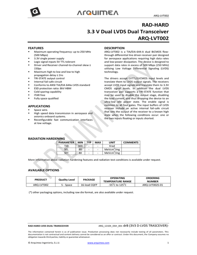
ARQ-LVT002 RAD-HARD 3.3 V Dual LVDS Dual Transceiver ARQ-LVT002 FEATURES DESCRIPTION ARQ-LVT002 is a TIA/EIA-644-A dual BiCMOS flowthrough differential line driver-receiver pair designed for aerospace applications requiring high data rates and low-power dissipation. The device is designed to support data rates in excess of 500 Mbps (250 MHz) utilizing Low Voltage Differential Signaling (LVDS) technology. Maximum operating frequency: up to 250 MHz (500 Mbps) 3.3V single power supply Logic signal inputs 5V TTL tolerant Driver and Receiver channel-to-channel skew ≤ 150ps Maximum high to low and low to high propagation delay ≤ 2ns TRI-STATE output control Internal fail-safe circuit Conforms to ANSI TIA/EIA 644a LVDS standard ESD protection ratio: 8kV HBM Cold sparing capability ITAR free Fully space qualified The drivers accept LVTTL/LVCMOS input levels and translate them to LVDS output signals. The receivers accept LVDS input signals and translate them to 3.3V CMOS signal levels. In addition the dual LVDS transceiver pair supports a TRI-STATE function that may be used to disable the output stage, disabling the load current, and thus dropping the device to an ultra-low idle power state. The enable signal is common to all four gates. The input buffers of LVDS receiver include an active internal fail-safe circuit that sets the output of the receiver to a known high state when the following conditions occur: one or the two inputs floating or inputs shorted. APPLICATIONS Space wire. High speed data transmission in aerospace and avionics onboard systems. Reconfigurable fast communication interfaces at low voltage. RADIATION HARDENING PARAMETER TID SEL SET MIN 300 80 80 TYP - MAX - UNIT Krad MeVcm2/mg MeVcm2/mg COMMENTS More information about radiation hardening features and radiation test conditions is available under request. AVAILABLE OPTIONS PRODUCT Quality Level PACKAGE ARQ-LVT002 S - Space 16-lead CQFP OPERATING TEMPERATURE RANGE -55oC to 125oC ORDERING NUMBER ARQ-LVT002S-01 (*) other packaging options, including raw die format, are also available under request. RAD-HARD LVDS DUAL TRANSCEIVER ARQ_12104_DSH_001 drB (3V3 D-LVDS TRASCEIVER)- The information contained herein is as of publication issue. Production processing does not necessarily include testing of all parameters. This documentation is not contractual and content delivery cannot be considered as an offer or contract. Under this document, the Company assumes no obligation towards third parties, liability or guarantee whatsoever. © Arquimea Ingeniería, S.L.U. www.arquimea.com 1 ARQ-LVT002 ELECTRICAL CHARACTERISTICS PARAMETER SYMBOL MIN TYP MAX UNIT Differential Output Voltage |VOD| 247 350 454 mV Change in magnitude of VOD for complementary output states Δ VOD - 5 50 mV Offset voltage VOS 1.125 1.25 1.375 V Change in magnitude of VOS for complementary output states ΔVOS - 5 50 mV Output short circuit current IOS - 5 9 mA Differential output short circuit current IOSD - 5 9 mA (1) IOFF -30 ±5 30 μA IOZ -10 ±3 10 μA Differential input high threshold VHT - 40 - mV Differential input low threshold VLT - -40 - mV VCMR -4 - 5 V IIN -10 ±6 10 μA Input high voltage VIH 2 - 5 V Input low voltage VIL -0.3 - 0.8 V VOH - 3.3 - V VOL - 0.05 0.25 V Differential propagation delay high to low tPDHL - 1 2 ns Differential propagation delay low to high tPDLH - 1 2 ns tSKD1 - 50 150 ps fMAX - 200 250 MHz Output Drivers Power-off Leakage Output TRI-STATE current Input Receiver Common-mode voltage range Input current Digital Input/Output Output high voltage Output low voltage (1) Driver switching characteristics Differential channel-to-channel skew (1) Maximum operating frequency Receiver switching characteristics Differential propagation delay high to low (2) tPDHL - 4.3 5 ns Differential propagation delay low to high (2) tPDLH - 4.3 5 ns tSKD1 - 50 150 ps fMAX - 200 250 MHz Differential channel-to-channel skew Maximum operating frequency (1) (1) Estimated value (2) Values obtained with the current CMOS logic output pads. These values will be reduced to 2ns max when the new bipolar-based CMOS pads are completed. RAD-HARD LVDS DUAL TRANSCEIVER ARQ_12104_DSH_001 drB (3V3 D-LVDS TRASCEIVER)- The information contained herein is as of publication issue. Production processing does not necessarily include testing of all parameters. This documentation is not contractual and content delivery cannot be considered as an offer or contract. Under this document, the Company assumes no obligation towards third parties, liability or guarantee whatsoever. © Arquimea Ingeniería, S.L.U. www.arquimea.com 2 ARQ-LVT002 PINOUT DESCRIPTION № pin PIN Name Type Direction Description 1 RIN1- Input A Input negative port of receiver R1, LVDS level 2 RIN1+ Input A Input positive port of receiver R1, LVDS level 3 RIN2+ Input A Input positive port of receiver R2, LVDS level 4 RIN2- Input A Input negative port of receiver R2, LVDS level 5 DOUT2- Output A Output negative port of driver D2, LVDS level 6 DOUT2+ Output A Output positive port of driver D2, LVDS level 7 DOUT1+ Output A Output positive port of driver D1, LVDS level 8 DOUT1- Output A Output negative port of driver D1, LVDS level 9 NC 10 DIN1 Input 11 DIN2 Input 12 VDD PWR Supply voltage 13 GND GND Ground 14 ROUT2 Output D Output data of receiver R2 15 ROUT1 Output D Output data of receiver R1 16 EN Input D Enable RAD-HARD LVDS DUAL TRANSCEIVER No Connection D Input data for driver D1 D Input data for driver D2 ARQ_12104_DSH_001 drB (3V3 D-LVDS TRASCEIVER)- The information contained herein is as of publication issue. Production processing does not necessarily include testing of all parameters. This documentation is not contractual and content delivery cannot be considered as an offer or contract. Under this document, the Company assumes no obligation towards third parties, liability or guarantee whatsoever. © Arquimea Ingeniería, S.L.U. www.arquimea.com 3 ARQ-LVT002 BLOCK DIAGRAM TYPICAL APPLICATION RAD-HARD LVDS DUAL TRANSCEIVER ARQ_12104_DSH_001 drB (3V3 D-LVDS TRASCEIVER)- The information contained herein is as of publication issue. Production processing does not necessarily include testing of all parameters. This documentation is not contractual and content delivery cannot be considered as an offer or contract. Under this document, the Company assumes no obligation towards third parties, liability or guarantee whatsoever. © Arquimea Ingeniería, S.L.U. www.arquimea.com 4 ARQ-LVT002 RADIATION TEST PERFORMANCE Radiation test vehicles are sub-circuits of the full device that are used to facilitate testing of their radiation compliance. They include the critical parts of the chip, in order to get insight on the circuit performance after irradiation. Proper radiation test vehicles have been carried out for validating radiation requirements of the key parameters of the ARQ-LVT002, in any radiation environment by any potential user. In a first step, a full test chip will has been designed and fabricated to allow a comprehensive characterization of the radiation degradation of the circuit blocks. Critical circuit parameters have been monitored after radiation up to several irradiation steps in order to observe the progressive degradation. The aim of the test chip with regard to radiation is to gain a better understanding of the circuit performance degradation due to the degradation of its constituents. It also gives designers a more accurate knowledge of the ranges of variation of the critical circuit parameters, for the target radiation levels, so that they can make their designs more robust against those variations at less expense in the general circuit complexity and performance. In a second step, some of the most representative test vehicles for the radiation degradation of the full circuit performance have been implemented in the ARQ-LVT002 device. This way the radiation performance of the full blocks can be evaluated with simple tests with the use of these test vehicles. Furthermore, the test vehicles included in the device give better understanding on the general block degradation for different radiation environments. More information about radiation tests and mitigation techniques for Total Ionizing Dose effects, Single Event Latch-up and Single Event Upsets, is available under request. QUALITY STANDARDS ARQUIMEA INGENIERÍA S.L.U. develops its activities under the premises of quality and sustainability, offering efficient, liable and innovative technologies and solutions to its customers. product line according to military and space standards. ARQUIMEA’s Quality Management System meets the requirements of ISO 9100:2010 Aerospace Series, and has been audited and certified by the Spanish Association for Standardization and Certification, AENOR. In order to meet the highest quality and reliability, ARQUIMEA designs and develops its aerospace RAD-HARD LVDS DUAL TRANSCEIVER ARQ_12104_DSH_001 drB (3V3 D-LVDS TRASCEIVER)- The information contained herein is as of publication issue. Production processing does not necessarily include testing of all parameters. This documentation is not contractual and content delivery cannot be considered as an offer or contract. Under this document, the Company assumes no obligation towards third parties, liability or guarantee whatsoever. © Arquimea Ingeniería, S.L.U. www.arquimea.com 5 ARQ-LVT002 IMPORTANT NOTICE ARQUIMEA INGENIERÍA S.L.U. and its subsidiaries (ARQUIMEA) reserve the right to make corrections, modifications, enhancements, improvements, and other changes to its products and services at any time and to discontinue any product or service without notice. Customers must obtain the latest relevant information before placing orders and must verify that such information is current and complete. All products are sold subject to ARQUIMEA’s terms and conditions of sale supplied at the time of order acknowledgment. ARQUIMEA warrants performance of its hardware products to the specifications applicable at the time of sale in accordance with ARQUIMEA’s standard warranty. Testing and other quality control techniques are used to the extent ARQUIMEA deems necessary to support this warranty. Except where mandated by legal requirements, testing of all parameters of each product is not necessarily performed. ARQUIMEA assumes no liability for applications assistance or customer product design. Customers are responsible for their products and applications using ARQUIMEA components. To minimize the risks associated with customer products and applications, customers should provide adequate design and operating safeguards. ARQUIMEA does not warrant or represent that any license, either express or implied, is granted under any ARQUIMEA patent right, copyright, mask work right, or other ARQUIMEA intellectual property right relating to any combination, machine, or process in which ARQUIMEA products or services are used. Information published by ARQUIMEA regarding third-party products or services does not constitute a license from ARQUIMEA to use such products or services or a warranty or endorsement thereof. Use of such information may require a license from a third party under the patents or other intellectual property of the third party, or a license from ARQUIMEA under the patents or other intellectual property of ARQUIMEA. Reproduction of ARQUIMEA information in ARQUIMEA data books or data sheets is permissible only if reproduction is without alteration and is accompanied by all associated warranties, conditions, limitations, and notices. Reproduction of this information with alteration is an unfair and deceptive business practice. ARQUIMEA is not responsible or liable for such altered documentation. Information of third parties may be subject to additional restrictions. Resale of ARQUIMEA products or services with statements different from or beyond the parameters stated by ARQUIMEA for that product or service voids all express and any implied warranties for the associated ARQUIMEA product or service and is an unfair and deceptive business practice. ARQUIMEA is not responsible or liable for any such statements. ARQUIMEA products are not authorized for use in safety-critical applications (such as life support) where a failure of the ARQUIMEA product would reasonably be expected to cause severe personal injury or death, unless officers of the parties have executed an agreement specifically governing such use. Buyers represent that they have all necessary expertise in the safety and regulatory ramifications of their applications, and acknowledge and agree that they are solely responsible for all legal, regulatory and safety-related requirements concerning their products and any use of ARQUIMEA products in such safety-critical applications, notwithstanding any applications-related information or support that may be provided by ARQUIMEA. Further, Buyers must fully indemnify ARQUIMEA and its representatives against any damages arising out of the use of ARQUIMEA products in such safety-critical applications. Only products designated by ARQUIMEA as military-grade or space-grade meet military or space specifications. Buyers acknowledge and agree that any such use of ARQUIMEA products which ARQUIMEA has not designated as military-grade or space-grade is solely at the Buyer's risk and that they are solely responsible for compliance with all legal and regulatory requirements in connection with such use. RAD-HARD LVDS DUAL TRANSCEIVER ARQ_12104_DSH_001 drB (3V3 D-LVDS TRASCEIVER)- The information contained herein is as of publication issue. Production processing does not necessarily include testing of all parameters. This documentation is not contractual and content delivery cannot be considered as an offer or contract. Under this document, the Company assumes no obligation towards third parties, liability or guarantee whatsoever. © Arquimea Ingeniería, S.L.U. www.arquimea.com 6
