®
RT5795A
2A, 5.5V, Low IQ ACOT Synchronous Step-Down Converter
General Description
Features
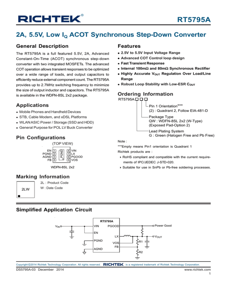
The RT5795A is a full featured 5.5V, 2A, Advanced
Constant-On-Time (ACOT) synchronous step-down
converter with two integrated MOSFETs. The advanced
COT operation allows transient responses to be optimized
over a wide range of loads, and output capacitors to
efficiently reduce external component count. The RT5795A
provides up to 2.7MHz switching frequency to minimize
the size of output inductor and capacitors. The RT5795A
is available in the WDFN-8SL 2x2 package.
2.5V to 5.5V Input Voltage Range
Advanced COT Control loop design
Fast Transient Response
Internal 100mΩ
Ω and 80mΩ
Ω Synchronous Rectifier
Highly Accurate VOUT Regulation Over Load/Line
Range
Robust Loop Stability with Low-ESR COUT
Ordering Information
RT5795A
Applications
Mobile Phones and Handheld Devices
STB, Cable Modem, and xDSL Platforms
WLAN ASIC Power / Storage (SSD and HDD)
General Purpose for POL LV Buck Converter
Pin 1 Orientation***
(2) : Quadrant 2, Follow EIA-481-D
Package Type
QW : WDFN-8SL 2x2 (W-Type)
(Exposed Pad-Option 2)
Lead Plating System
G : Green (Halogen Free and Pb Free)
Pin Configurations
Note :
EN
PGND
AGND
FB
PGND
(TOP VIEW)
1
2
3
4
9
8
7
6
5
***Empty means Pin1 orientation is Quadrant 1
VIN
LX
PGOOD
VOS
Richtek products are :
RoHS compliant and compatible with the current requirements of IPC/JEDEC J-STD-020.
WDFN-8SL 2x2
Suitable for use in SnPb or Pb-free soldering processes.
Marking Information
2L : Product Code
2LW
W : Date Code
Simplified Application Circuit
RT5795A
VIN
VIN
Power Good
PGOOD
EN
VOUT
LX
PGND
AGND
VOS
FB
R1
R2
Copyright © 2014 Richtek Technology Corporation. All rights reserved.
DS5795A-03 December 2014
is a registered trademark of Richtek Technology Corporation.
www.richtek.com
1
RT5795A
Functional Pin Description
Pin No.
Pin Name
1
EN
2,
PGND
9 (Exposed Pad)
Pin Function
Enable Control Input. Pull High to Enable.
Power Ground. The exposed pad must be soldered to a large PCB and
connected to PGND for maximum power dissipation.
3
AGND
Analog Ground. Should be electrically connected to GND close to the device.
4
FB
Feedback Voltage Input.
5
VOS
Output Voltage Sense Pin for the Internal Control Loop. Must be connected to
output.
6
PGOOD
Power Good Open-Drain Output. This pin is pulled to low if the output voltage is
below regulation limits. Can be left floating if not used.
7
LX
Switch Node. The Source of the internal high-side power MOSFET, and Drain of
the internal low-side (synchronous) rectifier MOSFET.
8
VIN
Power Input Supply Voltage, 2.5V to 5.5V.
Function Block Diagram
VOS
EN
AGND
UVLO
Shutdown
Control
OTP
FB
TON
Error Amplifier
+
+
Comparator
+
-
VREF
Logic
Control
Ramp
Generator
Current
Limit
Detector
LX
AZC
LX
VIN
Driver
LX
LX
PGOOD
+
VFB
-
Copyright © 2014 Richtek Technology Corporation. All rights reserved.
www.richtek.com
2
LX
PGND
is a registered trademark of Richtek Technology Corporation.
DS5795A-03 December 2014
RT5795A
Operation
The RT5795A is a low voltage synchronous step-down
converter that can support input voltage ranging from 2.5V
to 5.5V and the output current can be up to 2A. The
RT5795A uses ACOTTM mode control. To achieve good
stability with low-ESR ceramic capacitors, the ACOT uses
a virtual inductor current ramp generated inside the IC.
This internal ramp signal replaces the ESR ramp normally
provided by the output capacitor's ESR. The ramp signal
and other internal compensations are optimized for lowESR ceramic output capacitors.
In steady-state operation, the feedback voltage, with the
virtual inductor current ramp added, is compared to the
reference voltage. When the combined signal is less than
the reference, the on-time one-shot is triggered, as long
as the minimum off-time one-shot is clear and the
measured inductor current (through the synchronous
rectifier) is below the current limit. The on-time one-shot
turns on the high-side switch and the inductor current
ramps up linearly. After the on-time, the high-side switch
is turned off and the synchronous rectifier is turned on
and the inductor current ramps down linearly. At the same
time, the minimum off-time one-shot is triggered to prevent
another immediate on-time during the noisy switching
time and allow the feedback voltage and current sense
signals to settle. The minimum off-time is kept short so
that rapidly-repeated on-times can raise the inductor
current quickly when needed.
PWM Frequency and Adaptive On-Time Control
Power Good
When the output voltage is higher than PGOOD rising
threshold, the PGOOD flag is high.
Output Under-Voltage Protection (UVP)
When the output voltage is lower than 66% reference
voltage after soft-start, the UVP is triggered.
Over-Current Protection (OCP)
The RT5795A senses the current signal when the highside and low-side MOSFET turns on. As a result, The
OCP is a cycle-by-cycle current limit. If an over-current
condition occurs, the converter turns off the next on pulse
until inductor current drops below the OCP limit. If the
OCP is continually activated and the load current is larger
than the current provided by the converter, the output
voltage drops. Also, when the output voltage triggers the
UVP also, the current will drop to ZC and trigger the resoft start sequence.
Soft-Start
An internal current source charges an internal capacitor
to build the soft-start ramp voltage. The typical soft-start
time is 150μs.
Over-Temperature Protection (OTP)
The RT5795A has an over-temperature protection. When
the device triggers the OTP, the device shuts down until
the temperature is back to normal.
The on-time can be roughly estimated by the equation :
V
1
TON = OUT
where fOSC is nominal 2.7MHz
VIN
fOSC
Under-Voltage Protection (UVLO)
The UVLO continuously monitors the VCC voltage to make
sure the device works properly. When the VCC is high
enough to reach the UVLO high threshold voltage, the
step-down converter softly starts or pre-bias to its regulated
output voltage. When the VCC decreases to its low
threshold voltage, the device shuts down.
Copyright © 2014 Richtek Technology Corporation. All rights reserved.
DS5795A-03 December 2014
is a registered trademark of Richtek Technology Corporation.
www.richtek.com
3
RT5795A
Absolute Maximum Ratings
(Note 1)
Supply Input Voltage, VIN ----------------------------------------------------------------------------------------Other Pins ------------------------------------------------------------------------------------------------------------Power Dissipation, PD @ TA = 25°C
WDFN-8SL 2x2 -----------------------------------------------------------------------------------------------------Package Thermal Resistance (Note 2)
WDFN-8SL 2x2, θJA ------------------------------------------------------------------------------------------------WDFN-8SL 2x2, θJC -----------------------------------------------------------------------------------------------Junction Temperature ----------------------------------------------------------------------------------------------Lead Temperature (Soldering, 10 sec.) ------------------------------------------------------------------------Storage Temperature Range -------------------------------------------------------------------------------------ESD Susceptibility (Note 3)
HBM (Human Body Model) ----------------------------------------------------------------------------------------
Recommended Operating Conditions
−0.3V to 6V
−0.3V to (VIN + 0.3V)
1.538W
65°C/W
8°C/W
150°C
260°C
−65°C to 150°C
2kV
(Note 4)
Supply Input Voltage, VIN ----------------------------------------------------------------------------------------- 2.5V to 5.5V
Junction Temperature Range -------------------------------------------------------------------------------------- −40°C to 125°C
Ambient Temperature Range -------------------------------------------------------------------------------------- −40°C to 85°C
Electrical Characteristics
(VIN = 3.6V, TA = 25°C, unless otherwise specified)
Parameter
Symbol
Test Conditions
Min
Typ
Max
Unit
2.28
2.35
2.48
V
--
400
--
mV
Under-Voltage Lockout
Threshold
VUVLO
Under-Voltage Lockout
Hysteresis
VUVLOHY
Shutdown Supply Current
ISHDN
EN = 0V
--
--
1
A
Quiescent Current
IQ
Active, VFB = 0.5V, No Switching
--
30
--
A
Voltage Reference
VREF
0.441
0.45
0.459
V
Peak Current
2.5
3.2
4
Valley Current
2
2.4
2.9
15
10
5
%
Current Limit
High-Side
Low-Side
ILIM
VCC Rising
A
Power Good Threshold
VPGTH
VOUT Falling Referenced to VOUT
Nominal
Power Good Hysteresis
VPGHY
Hysteresis Referenced to VOUT
Nominal
--
5
--
%
Power Good Leakage
Current
IPG
VPG = 5V
--
0.01
0.1
A
Power Good Low Level
Voltage
VPGL
Isink = 500A
--
--
0.3
V
Enable Rising Threshold
VENR
Rising
1
--
--
V
Enable Falling Threshold
VENF
Falling
--
--
0.4
V
Copyright © 2014 Richtek Technology Corporation. All rights reserved.
www.richtek.com
4
is a registered trademark of Richtek Technology Corporation.
DS5795A-03 December 2014
RT5795A
Parameter
Symbol
Test Conditions
Min
Typ
Max
Unit
High-Side
RP-MOSFET
--
100
--
Low-Side
RN-MOSFET
--
80
--
Thermal Shutdown
Temperature
--
150
--
C
Thermal Shutdown
Hysteresis
--
20
--
C
--
2.7
--
MHz
--
1
--
k
Switch
On-Resistance
Switching Frequency
fOSC
Output Discharge Resistor
m
Note 1. Stresses beyond those listed “Absolute Maximum Ratings” may cause permanent damage to the device. These are
stress ratings only, and functional operation of the device at these or any other conditions beyond those indicated in
the operational sections of the specifications is not implied. Exposure to absolute maximum rating conditions may
affect device reliability.
Note 2. θJA is measured at TA = 25°C on a high effective thermal conductivity four-layer test board per JEDEC 51-7. θJC is
measured at the exposed pad of the package. The copper area is 70mm2 connected with IC exposed pad.
Note 3. Devices are ESD sensitive. Handling precaution is recommended.
Note 4. The device is not guaranteed to function outside its operating conditions.
Copyright © 2014 Richtek Technology Corporation. All rights reserved.
DS5795A-03 December 2014
is a registered trademark of Richtek Technology Corporation.
www.richtek.com
5
RT5795A
Typical Application Circuit
RT5795A
8
VIN
10µF
VIN
PGOOD
1 EN
LX
2, 9 (Exposed Pad)
6
7
5
PGND
3 AGND
VOS
FB 4
Power Good
180k
L
VOUT
R1
COUT
R2
Table 1. Suggested Component Values
VOUT (V)
R1 (k)
R2 (k)
L (H)
COUT (F)
1.2V
65.3
39.2
0.47
22
1.8V
117.6
39.2
1
22
2.5V
178.6
39.2
1
22
3.3V
248.3
39.2
1
22
Copyright © 2014 Richtek Technology Corporation. All rights reserved.
www.richtek.com
6
is a registered trademark of Richtek Technology Corporation.
DS5795A-03 December 2014
RT5795A
Typical Operating Characteristics
Efficiency vs. Output Current
Efficiency vs. Output Current
100
100
90
90
80
80
VIN = 3.3V
VIN = 5V
60
Efficiency (%)
Efficiency (%)
70
50
40
30
70
VIN = 3.3V
VIN = 5V
60
50
40
30
20
20
10
10
VOUT = 1.2V, L = 0.47μH
0
0.001
VOUT = 1.2V, L = 0.47μH
0
0.01
0.1
1
0
10
0.5
Efficiency vs. Output Current
2
Efficiency vs. Output Current
100
100
90
90
VIN = 3.3V
VIN = 5V
80
VIN = 3.3V
VIN = 5V
80
Efficiency (%)
70
Efficiency (%)
1.5
Output Current (A)
Output Current (A)
60
50
40
30
20
70
60
50
40
30
20
10
10
VOUT = 2.5V, L = 1μH
0
0.001
VOUT = 2.5V, L = 1μH
0
0.01
0.1
1
10
0
0.5
Output Current (A)
1.240
2.58
1.230
2.56
Output Voltage (V)
2.60
1.220
VIN = 5V
VIN = 3.3V
1.200
1.5
2
Output Voltage vs. Output Current
1.250
1.210
1
Output Current (A)
Output Voltage vs. Output Current
Output Voltage(V)
1
1.190
1.180
1.170
2.54
VIN = 5V
VIN = 3.3V
2.52
2.50
2.48
2.46
2.44
1.160
2.42
VOUT = 1.2V, L = 0.47μH
1.150
VOUT = 2.5V, L = 1μH
2.40
0
0.5
1
1.5
Output Current (A)
Copyright © 2014 Richtek Technology Corporation. All rights reserved.
DS5795A-03 December 2014
2
0
0.5
1
1.5
2
Output Current (A)
is a registered trademark of Richtek Technology Corporation.
www.richtek.com
7
RT5795A
Output Voltage vs. Input Voltage
2.54
1.215
2.53
2.52
1.210
Output Voltage (V)
Output Voltage (V)
Output Voltage vs. Input Voltage
1.220
1.205
1.200
1.195
1.190
2.51
2.50
2.49
2.48
2.47
2.46
1.185
2.45
VOUT = 1.2V, IOUT = 0A, L = 0.47μH
1.180
VOUT = 2.5V, IOUT = 0A, L = 1μH
2.44
2.5
3
3.5
4
4.5
5
5.5
2.5
3
3.5
Input Voltage (V)
5
5.5
Switching Frequency vs. Temperature
3.0
2.9
2.9
Switching Frequency (MHz)1
Switching Frequency (MHz)1
Switching Frequency vs. Input Voltage
2.8
2.7
2.6
2.5
2.4
2.3
2.2
VOUT = 1.2V, IOUT = 0A, L = 0.47μH
2.0
2.8
2.7
2.6
2.5
2.4
2.3
2.2
2.1
VIN = 5V, VOUT = 1.2V, IOUT = 1A, L = 0.47μH
2.0
2.5
3
3.5
4
4.5
5
5.5
-50
-25
0
Input Voltage (V)
50
75
100
125
Output Current Limit vs. Temperature
4.0
3.8
3.8
Output Current Limit (A)
4.0
3.6
3.4
3.2
3.0
2.8
2.6
2.4
2.2
25
Temperature (°C)
Output Current Limit vs. Input Voltage
Output Current Limit (A)
4.5
Input Voltage (V)
3.0
2.1
4
VOUT = 1.2V, L = 0.47μH
2.0
3.6
3.4
3.2
3.0
2.8
2.6
2.4
2.2
VIN = 3.3V, VOUT = 1.2V, L = 0.47μH
2.0
2.5
3
3.5
4
4.5
5
Input Voltage (V)
Copyright © 2014 Richtek Technology Corporation. All rights reserved.
www.richtek.com
8
5.5
-50
-25
0
25
50
75
100
125
Temperature (°C)
is a registered trademark of Richtek Technology Corporation.
DS5795A-03 December 2014
RT5795A
Input Voltage vs. Temperature
Enable Threshold vs. Temperature
2.5
2.0
2.4
1.8
UVLO Turn On
1.6
Enable Voltage (V)
Input Voltage (V)
2.3
2.2
2.1
2.0
1.9
UVLO Turn Off
1.8
1.4
1.2
0.8
Enable Off
0.6
1.7
0.4
1.6
0.2
1.5
Enable On
1.0
0.0
-50
-25
0
25
50
75
100
125
-50
-25
0
25
50
75
100
Temperature (°C)
Temperature (°C)
Load Transient Response
Load Transient Response
VOUT
(20mV/Div)
VOUT
(20mV/Div)
IOUT
(1A/Div)
IOUT
(1A/Div)
VIN = 5V, VOUT = 2.5V, IOUT = 1A to 2A, L = 1μH
VIN = 5V, VOUT = 2.5V, IOUT = 0A to 2A, L = 1μH
Time (50μs/Div)
Time (50μs/Div)
Load Transient Response
Load Transient Response
VOUT
(20mV/Div)
VOUT
(20mV/Div)
IOUT
(1A/Div)
IOUT
(1A/Div)
VIN = 3.3V, VOUT = 1.2V, IOUT = 1A to 2A, L = 0.47μH
Time (50μs/Div)
Copyright © 2014 Richtek Technology Corporation. All rights reserved.
DS5795A-03 December 2014
125
VIN = 3.3V, VOUT = 1.2V, IOUT = 0A to 2A, L = 0.47μH
Time (50μs/Div)
is a registered trademark of Richtek Technology Corporation.
www.richtek.com
9
RT5795A
Voltage Ripple
Voltage Ripple
VOUT
(20mV/Div)
VOUT
(20mV/Div)
VLX
(5V/Div)
VLX
(5V/Div)
VIN = 3.3V, VOUT = 1.2V, IOUT = 2A, L = 0.47μH
VIN = 3.3V, VOUT = 1.2V, IOUT = 1A, L = 0.47μH
Time (500ns/Div)
Time (500ns/Div)
Voltage Ripple
Voltage Ripple
VOUT
(20mV/Div)
VOUT
(20mV/Div)
VLX
(5V/Div)
VLX
(5V/Div)
VIN = 5V, VOUT = 2.5V, IOUT = 2A, L = 1μH
VIN = 5V, VOUT = 2.5V, IOUT = 1A, L = 1μH
Time (500ns/Div)
Time (500ns/Div)
Power On from VIN
Power Off from VIN
VEN
(5V/Div)
VEN
(5V/Div)
VOUT
(1V/Div)
VLX
(5V/Div)
VOUT
(1V/Div)
VLX
(5V/Div)
IOUT
(2A/Div)
IOUT
(2A/Div)
VIN = 5V, VOUT = 1.2V, IOUT = 2A
Time (100μs/Div)
Copyright © 2014 Richtek Technology Corporation. All rights reserved.
www.richtek.com
10
VIN = 5V, VOUT = 1.2V, IOUT = 2A
Time (100μs/Div)
is a registered trademark of Richtek Technology Corporation.
DS5795A-03 December 2014
RT5795A
Application Information
The RT5795A is a single-phase step-down converter.
Advance Constant-on-Time (ACOT) with fast transient
response. An internal 0.45V reference allows the output
voltage to be precisely regulated for low output voltage
applications. A fixed switching frequency (2.7MHz)
oscillator and internal compensation are integrated to
minimize external component count. Protection features
include over current protection, under voltage protection
and over temperature protection.
Output Voltage Setting
The output voltage is set by an external resistive divider
according to the following equation :
R1
VOUT VREF x (1
)
R2
where VREF equals to 0.45V typical. The resistive divider
allows the FB pin to sense a fraction of the output voltage
as shown in Figure 1.
VOUT
R1
FB
RT5795A
R2
will retry automatically. When the UVP condition is
removed, the converter will resume operation. The UVP
is disabled during soft-start period.
Post Short
VIN
(2V/Div)
VOUT
(500mV/Div)
SW
(5V/Div)
IOUT
(2A/Div)
VIN = 5V, VOUT = 1.2V, L = 1μH
Time (1ms/Div)
CIN and COUT Selection
The input capacitance, C IN, is needed to filter the
trapezoidal current at the source of the top MOSFET. To
prevent large ripple voltage, a low ESR input capacitor
sized for the maximum RMS current should be used. RMS
current is given by :
GND
Figure 1. Setting the Output Voltage
Low Supply Operation
The RT5795A is designed to operate down to an input
supply voltage of 2.5V. One important consideration at
low input supply voltages is that the RDS(ON) of the PChannel and N-Channel power switches increases. The
user should calculate the power dissipation when the
RT5795A is used at 100% duty cycle with low input
voltages to ensure that thermal limits are not exceeded.
Under Voltage Protection (UVP)
Hiccup Mode
For the RT5795A, it provides Hiccup Mode Under Voltage
Protection (UVP). When the output voltage is lower than
66% reference voltage after soft-start, the UVP is triggered.
If the UVP condition remains for a period, the RT5795A
Copyright © 2014 Richtek Technology Corporation. All rights reserved.
DS5795A-03 December 2014
IRMS IOUT(MAX)
VOUT
VIN
VIN
1
VOUT
This formula has a maximum at VIN = 2VOUT, where IRMS =
IOUT / 2. This simple worst case condition is commonly
used for design because even significant deviations do
not result in much difference. Choose a capacitor rated at
a higher temperature than required.
Several capacitors may also be paralleled to meet size or
height requirements in the design.
The selection of COUT is determined by the effective series
resistance (ESR) that is required to minimize voltage ripple
and load step transients, as well as the amount of bulk
capacitance that is necessary to ensure that the control
loop is stable. Loop stability can be checked by viewing
the load transient response. The output ripple, ΔVOUT, is
determined by :
1
VOUT IL ESR
8fCOUT
is a registered trademark of Richtek Technology Corporation.
www.richtek.com
11
RT5795A
The high Q of ceramic capacitors with trace inductance
can also lead to significant ringing.
Using Ceramic Input and Output Capacitors
Higher value, lower cost ceramic capacitors are now
becoming available in smaller case sizes. Their high ripple
current, high voltage rating and low ESR make them ideal
for switching regulator applications. However, care must
be taken when these capacitors are used at the input and
output. When a ceramic capacitor is used at the input
and the power is supplied by a wall adapter through long
wires, a load step at the output can induce ringing at the
input, VIN. At best, this ringing can couple to the output
and be mistaken as loop instability. At worst, a sudden
inrush of current through the long wires can potentially
cause a voltage spike at VIN large enough to damage the
part.
Table 2. Capacitors for CIN and COUT
Component
Supplier
Part No.
Capacitance Case
(F)
Size
MuRata
GRM31CR71A106KA01
10F
1206
MuRata
GRM31CR71A226KA01
22F
1206
Thermal Considerations
For continuous operation, do not exceed absolute
maximum junction temperature. The maximum power
dissipation depends on the thermal resistance of the IC
package, PCB layout, rate of surrounding airflow, and
difference between junction and ambient temperature. The
maximum power dissipation can be calculated by the
following formula :
PD(MAX) = (TJ(MAX) − TA) / θJA
where TJ(MAX) is the maximum junction temperature, TA is
the ambient temperature, and θJA is the junction to ambient
thermal resistance.
For recommended operating condition specifications, the
maximum junction temperature is 125°C. The junction to
ambient thermal resistance, θJA, is layout dependent. The
junction to ambient thermal resistance, θJA, is layout
dependent. For WDFN-8SL 2x2 packages, the thermal
resistance, θJA, is 65°C/W on a standard JEDEC 51-7
four-layer thermal test board. The maximum power
dissipation at TA = 25°C can be calculated by the following
formula :
PD(MAX) = (125°C − 25°C) / (65°C/W) = 1.538W for
WDFN-8SL 2x2 package
The maximum power dissipation depends on the operating
ambient temperature for fixed T J(MAX) and thermal
resistance, θJA. The derating curve in Figure 2 allows the
designer to see the effect of rising ambient temperature
on the maximum power dissipation.
2.0
Maximum Power Dissipation (W)1
The output ripple is highest at maximum input voltage
since ΔIL increases with input voltage. Multiple capacitors
placed in parallel may be needed to meet the ESR and
RMS current handling requirements. Dry tantalum, special
polymer, aluminum electrolytic and ceramic capacitors are
all available in surface mount packages. Special polymer
capacitors offer very low ESR, but have lower capacitance
density than other types. Tantalum capacitors have the
highest capacitance density, but it is important to only
use types that have been surge tested for use in switching
power supplies. Aluminum electrolytic capacitors have
significantly higher ESR, but can be used in cost-sensitive
applications provided that consideration is given to ripple
current ratings and long term reliability. Ceramic capacitors
have excellent low ESR characteristics, but can have a
high voltage coefficient and audible piezoelectric effects.
Four-Layer PCB
1.6
1.2
0.8
0.4
0.0
0
25
50
75
100
125
Ambient Temperature (°C)
Figure 2. Derating Curve of Maximum Power Dissipation
Copyright © 2014 Richtek Technology Corporation. All rights reserved.
www.richtek.com
12
is a registered trademark of Richtek Technology Corporation.
DS5795A-03 December 2014
RT5795A
Layout Considerations
Flood all unused areas on all layers with copper. Flooding
Follow the PCB layout guidelines for optimal performance
of the RT5795A.
with copper will reduce the temperature rise of power
components. Connect the copper areas to any DC net
(VIN, VOUT, GND, or any other DC rail in the system).
Connect the terminal of the input capacitor(s), CIN, as
close as possible to the VIN pin. This capacitor provides
the AC current into the internal power MOSFETs.
LX node experiences high frequency voltage swing and
should be kept within a small area. Keep all sensitive
small-signal nodes away from the LX node to prevent
stray capacitive noise pick up.
Connect the FB pin directly to the feedback resistors.
The resistive voltage divider must be connected between
VOUT and GND.
Input capacitor must be placed
as close to the IC as possible.
GND CIN
VIN
LX should be connected to inductor by
wide and short trace. Keep sensitive
components away from this trace
R2
EN
PGND
AGND
FB
1
2
3
4
PGND
CIN
9
8
7
6
5
VIN
LX
PGOOD
VOS
COUT
L
R1
COUT
VOUT
VOUT
The feedback and must be connected as close to the
device as possible. Keep sensitive component away.
Figure 3. PCB Layout Guide
Copyright © 2014 Richtek Technology Corporation. All rights reserved.
DS5795A-03 December 2014
is a registered trademark of Richtek Technology Corporation.
www.richtek.com
13
RT5795A
Outline Dimension
2
1
2
1
DETAIL A
Pin #1 ID and Tie Bar Mark Options
Note : The configuration of the Pin #1 identifier is optional,
but must be located within the zone indicated.
Symbol
Dimensions In Millimeters
Dimensions In Inches
Min.
Max.
Min.
Max.
A
0.700
0.800
0.028
0.031
A1
0.000
0.050
0.000
0.002
A3
0.175
0.250
0.007
0.010
b
0.200
0.300
0.008
0.012
D
1.900
2.100
0.075
0.083
Option1
1.150
1.250
0.045
0.049
Option2
1.550
1.650
0.061
0.065
E
1.900
2.100
0.075
0.083
Option1
0.750
0.850
0.030
0.033
Option2
0.850
0.950
0.033
0.037
D2
E2
e
L
0.500
0.250
0.020
0.350
0.010
0.014
W-Type 8SL DFN 2x2 Package
Richtek Technology Corporation
14F, No. 8, Tai Yuen 1st Street, Chupei City
Hsinchu, Taiwan, R.O.C.
Tel: (8863)5526789
Richtek products are sold by description only. Richtek reserves the right to change the circuitry and/or specifications without notice at any time. Customers should
obtain the latest relevant information and data sheets before placing orders and should verify that such information is current and complete. Richtek cannot
assume responsibility for use of any circuitry other than circuitry entirely embodied in a Richtek product. Information furnished by Richtek is believed to be
accurate and reliable. However, no responsibility is assumed by Richtek or its subsidiaries for its use; nor for any infringements of patents or other rights of third
parties which may result from its use. No license is granted by implication or otherwise under any patent or patent rights of Richtek or its subsidiaries.
www.richtek.com
14
DS5795A-03 December 2014
