Considerations for Designing Power Electronic Devices Based on
Advanced SiC Technologies
By Mark Loboda, Chief Scientist-Compound Semiconductors, Dow Corning Electronics Solutions
Improvements in crystal quality
Growth of SiC crystals is generally performed through
sublimation (physical vapor transport) or chemical vapor
deposition. Specific methodologies to control defect densities
in large crystals are proprietary and closely guarded secrets.
Since 2009, publications by the State University of New York
and Dow Corning have demonstrated significant progress in
the reduction of dislocations in SiC1. Dow Corning is now
exploiting these defect reduction methods in recent efforts to
supply 150-mm diameter substrates to the market.
Thus, even at mainstream production volumes, 150-mm
diameter SiC wafers are an expensive platform for device
development, especially if the quality is poor. So, to take full
advantage of large substrates, wafer makers must support high
production yields by minimizing defects in the material – or at
least maintaining defect densities offered by smaller wafers. In
addition, the performance of epitaxial film parameters and the
device fabrication process must also be sufficient to use the
entire 150-mm wafer surface.
1
Darren Hansen, M.J. Loboda, Roman Drachev, Edward Sanchez, Jie Zhang,
Eric P Carlson, Jianwei Wan and Gil Chung (2010). Defect Reduction in SiC
Growth Using Physical Vapor Transport. MRS Proceedings, 1246 , 1246B01-04 doi:10.1557/PROC-1246-B01-04.
M. Dudley, S. Byrappa, H. Wang, F. Wu, Y. Zhang, B. Raghothamachar, G.
Choi, E. K. Sanchez, D. Hansen, R. Drachev, and M.J. Loboda,Analysis of
Dislocation Behavior in Low Dislocation Density, PVT-Grown, Four-Inch
Silicon Carbide Single Crystals, Material Research Symposium, San
Francisco, CA, April 4-9, 2010.
M. Dudley, S. Byrappa, H. Wang, F. Wu, Y. Zhang, B. Raghothamachar, G.
Choi, E. K. Sanchez, D. Hansen, R. Drachev, and M.J. Loboda,
Characterization of 100 mm Diameter 4H-Silicon Carbide Crystals With
Extremely Low Basal Plane Dislocation Density, Materials Science Forum,
645-648, (2010) p.291.
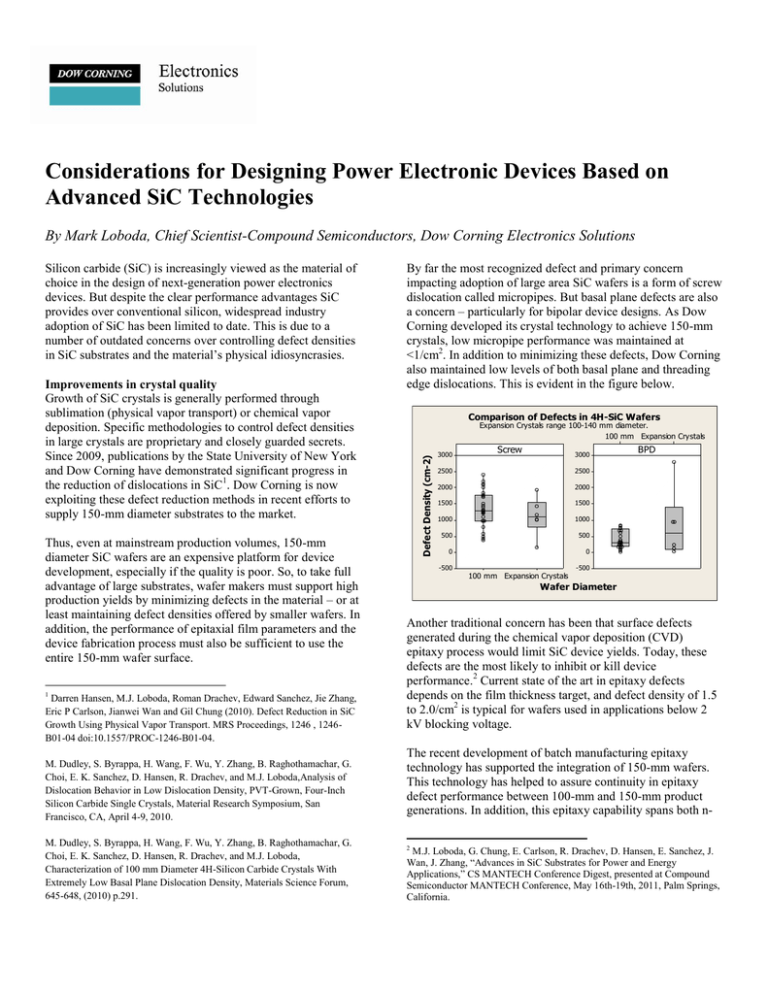
By far the most recognized defect and primary concern
impacting adoption of large area SiC wafers is a form of screw
dislocation called micropipes. But basal plane defects are also
a concern – particularly for bipolar device designs. As Dow
Corning developed its crystal technology to achieve 150-mm
crystals, low micropipe performance was maintained at
<1/cm2. In addition to minimizing these defects, Dow Corning
also maintained low levels of both basal plane and threading
edge dislocations. This is evident in the figure below.
Comparison of Defects in 4H-SiC Wafers
Expansion Crystals range 100-140 mm diameter.
100 mm Expansion Crystals
Defect Density (cm-2)
Silicon carbide (SiC) is increasingly viewed as the material of
choice in the design of next-generation power electronics
devices. But despite the clear performance advantages SiC
provides over conventional silicon, widespread industry
adoption of SiC has been limited to date. This is due to a
number of outdated concerns over controlling defect densities
in SiC substrates and the material’s physical idiosyncrasies.
3000
Screw
3000
2500
2500
2000
2000
1500
1500
1000
1000
500
500
0
0
-500
-500
100 mm Expansion Crystals
BPD
Wafer Diameter
Another traditional concern has been that surface defects
generated during the chemical vapor deposition (CVD)
epitaxy process would limit SiC device yields. Today, these
defects are the most likely to inhibit or kill device
performance.2 Current state of the art in epitaxy defects
depends on the film thickness target, and defect density of 1.5
to 2.0/cm2 is typical for wafers used in applications below 2
kV blocking voltage.
The recent development of batch manufacturing epitaxy
technology has supported the integration of 150-mm wafers.
This technology has helped to assure continuity in epitaxy
defect performance between 100-mm and 150-mm product
generations. In addition, this epitaxy capability spans both n2
M.J. Loboda, G. Chung, E. Carlson, R. Drachev, D. Hansen, E. Sanchez, J.
Wan, J. Zhang, “Advances in SiC Substrates for Power and Energy
Applications,” CS MANTECH Conference Digest, presented at Compound
Semiconductor MANTECH Conference, May 16th-19th, 2011, Palm Springs,
California.
and p-type dopants and the CVD process technology enables
thickness ranges to >50 microns for high-voltage applications.
These capabilities help promote 150-mm diameter substrate
technology in all types of SiC device design strategies.
Influences on SiC Device Cost
Once low defect densities have been achieved, the value of
larger SiC wafers becomes intuitive thanks to simple
geometry. To date, SiC device work has been based on 76-mm
and 100-mm diameter substrates. Compared to silicon devices
made on 150- to 200-mm diameter wafers, the cost to
manufacture devices on SiC substrates can be high due to the
SiC wafer cost plus the additional costs to accommodate
wafers of diameter smaller than 150 mm in the manufacturing
process flow. With the advent of 150-mm diameter SiC
substrates, device manufacturing costs can be reduced due to
the increase in substrate size (e.g. increased device count per
wafer fabrication pass). For device manufacturers who make
special efforts to use 100-mm diameter substrates today in a
manufacturing line designed for larger diameter wafers, there
is the potential for additional savings.
substrate with a larger number of die compared to a
conventional silicon power device design.
Clearly, as die count per wafer increases, costs should decline.
However, it is important to note that the relationship between
substrate costs and device manufacturing costs does not scale
directly when die size is a variable.
In simple terms for a fixed wafer diameter, the cost of the
epiwafer (Wafer$) combined with the cost to execute the
manufacturing and testing process (Fab$) represent the total
manufacturing costs. Good manufacturing economics require
that total costs taken relative to the number of dies per wafer
should be a constant:
(Wafer$ + Fab$)/(Device Count) = Constant
As the price of the wafer increases, Fab$ costs generally do
not change. Yet, with higher wafer price, the cost to
manufacture devices using SiC will also increase, unless a
larger die count is achieved.
Consider the equation:
(Wafer1$ + Fab$)/(Device Count1) = (Wafer2$ +
Fab$)/(Device Count2) = Constant
The potential manufacturing throughput requirements of SiC
can be estimated by considering the case for 150-mm wafer
diameters. For this example, Fab$=1000, silicon wafer
costs=$100 and the ratio of the SiC/Silicon wafer price cases
are 20x, 10x and 5x. This example is close to that for a power
transistor, and it illustrates the typical decline in new wafer
price as use volume increases.
Wafer Cost Ratio
20
10
5
That raises the question of whether or not SiC devices can be
manufactured at a cost point able to yield a device product that
is cost competitive with silicon power devices in system
applications. SiC’s properties enable design of power devices
with smaller area. This offers the opportunity to populate a
Relative Device Count for
Constant Device Cost
2.6
1.7
1.3
The column on the right above indicates the fractional increase
in the number of devices on a wafer, or the fractional
reduction in die area of the SiC device necessary to achieve
device fabrication cost parity with an equivalently specified
silicon device. The properties of SiC, particularly its thermal
conductivity, allow a device design strategy implementing a
2x reduction in die area. This calculation indicates that for Si
and SiC there can be a large differential in price between
wafers of the same size, but the cost to fabricate devices can
be comparable.
SiC Device Design and Fabrication
As high-crystal quality 150-mm SiC substrates achieve
commercial maturity over the next few quarters, examining
integration and design considerations will become more and
more important. Maximizing the benefits of SiC’s high
voltage and thermal conductivity properties (compared to
silicon) is critical to achieving successful device and system
designs. Awareness of other high-performance properties of
SiC wafers is also important in order to achieve successful
device performance:
Transparency. SiC wafers are transparent. This property
can lead to some difficulty in photolithography utilizing
steppers, in automated defect detection and in automated
wafer handling. Automated defect detection may
misidentify features below the surface as surface defects.
In wafer handling, sensors set up for opaque materials
may respond incorrectly, resulting in wafer breakage
during load/unload events.
Dopant Incorporation. Implantation and activation of
dopant atoms in SiC is more challenging than in silicon.
Dopant diffusion is extremely small compared to silicon.
Implant activation in SiC requires temperatures in excess
of 1500 C, and during this process the wafer surface must
be adequately protected to prevent roughening. Activation
efficiency may be lower than silicon, and total activation
varies with the total dopant concentration.
Substrate Resistivity. SiC substrates have higher
resistivity than silicon substrates. Since the epitaxy
thickness used in SiC designs is small compared to
silicon, the SiC substrate can contribute more to the series
resistance of a device. Ohmic contact formation on SiC
wafers often requires high temperature anneal (T>800 C).
This step must be performed early in the device
fabrication flow since the anneal temperature may be
detrimental to subsequent device processes. Process
optimization is important to assure series resistance
effects resulting from the ohmic contact are minimized,
and optimum low forward voltage drop performance in
SiC diodes and metal-oxide semiconductor field-effect
transistors (MOSFETs) is achieved.
Defects. The most critical defect associated with SiC
devices are polycrystalline surface defects that form on
the wafer surface during epitaxy. These killer defects are
easily detected with automated optical spectrometry
techniques. Surface protrusion from defects can lead to
comet formation in photoresist layers, and result in
fabrication failures in areas of the wafer away from the
defect. Inspection of photoresist is an important inprocess step to identify potential fabrication issues. Other
defects can also be present that can limit the performance
of devices. Very light damage from polishing processes
can result in shallow linear defects on the epitaxy surface
that will become decorated during metallization steps.
These defects can lead to hot spots on the device in the
region under the gate or in the edge termination areas.
Device Attributes. SiC devices like Schottky diodes and
MOSFETs exhibit positive temperature coefficients for
the forward bias on state resistance. Many results have
been reported in the literature and the device suppliers’
application notes that SiC devices exhibit lower
conduction losses and switching losses compared to
silicon-based devices. There are many models used when
designing SiC devices. But the models, while improving,
still show offsets from experimental data measured on
fabricated devices. Care should be made to ensure
materials properties entered in the model are consistent
with those of the materials used to fabricate the devices.
The model should be evaluated such that it reflects
internal wafer and wafer-to-wafer variations of the
substrate and epitaxy to provide leading indication of the
distribution of results.
Summary
The outstanding properties of SiC are recognized as being
advantageous for fabrication of power devices. Substrate costs
and defect densities are now continuously decreasing. While
not yet as mature and consistent as silicon, improvements
continue and significant progress is underway to more fully
understand the cause-and-effect relationships between the
variations and defects in SiC substrates and devices. Through
numerous collaborations and partnerships focused on the
materials characterization and device fabrication, expertise in
product specification and application development can
accelerate the efforts of semiconductor device manufacturers
to implement SiC in next-generation power devices and
systems.
Learn More
To find out how Dow Corning can support your power
electronics applications visit
dowcorning.com/powerelectronics or email us at
electronics@dowcorning.com.
LIMITED WARRANTY INFORMATION–PLEASE
READ CAREFULLY
The information contained herein is offered in good faith and
is believed to be accurate. However, because conditions and
methods of use of our products are beyond our control, this
information should not be used in substitution for customer’s
tests to ensure that our products are safe, effective and fully
satisfactory for the intended end use. Suggestions of use shall
not be taken as inducements to infringe any patent.
Dow Corning’s sole warranty is that our products will meet
the sales specifications in effect at the time of shipment.
Your exclusive remedy for breach of such warranty is limited
to refund of purchase price or replacement of any product
shown to be other than as warranted.
DOW CORNING SPECIFICALLY DISCLAIMS ANY
OTHER EXPRESS OR IMPLIED WARRANTY OF
FITNESS FOR A PARTICULAR PURPOSE OR
MERCHANTABILITY.
DOW CORNING DISCLAIMS LIABILITY FOR ANY
INCIDENTAL OR CONSEQUENTIAL DAMAGES.
Dow Corning is a registered trademark of Dow Corning
Corporation. We help you invent the future is a trademark of
Dow Corning Corporation.
©2013 Dow Corning Corporation. All rights reserved.
Form No. 11-3382


