Datasheet
AS1716
C a pa c i t i v e S e n s o r I n t e r f a c e
1 General Description
2 Key Features
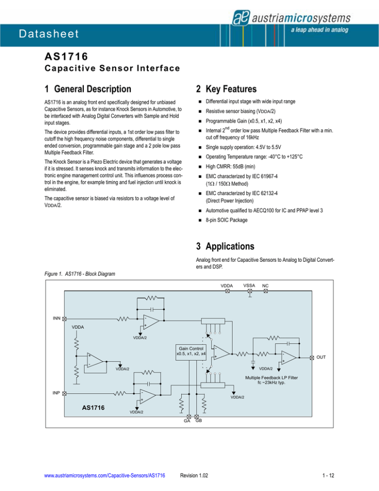
AS1716 is an analog front end specifically designed for unbiased
Capacitive Sensors, as for instance Knock Sensors in Automotive, to
be interfaced with Analog Digital Converters with Sample and Hold
input stages.
Differential input stage with wide input range
The device provides differential inputs, a 1st order low pass filter to
cutoff the high frequency noise components, differential to single
ended conversion, programmable gain stage and a 2 pole low pass
Multiple Feedback Filter.
Internal 2 order low pass Multiple Feedback Filter with a min.
cut off frequency of 16kHz
Resistive sensor biasing (VDDA/2)
Programmable Gain (x0.5, x1, x2, x4)
nd
Single supply operation: 4.5V to 5.5V
Operating Temperature range: -40°C to +125°C
The Knock Sensor is a Piezo Electric device that generates a voltage
if it is stressed. It senses knock and transmits information to the electronic engine management control unit. This influences process control in the engine, for example timing and fuel injection until knock is
eliminated.
High CMRR: 55dB (min)
EMC characterized by IEC 61967-4
(1Ω / 150Ω Method)
EMC characterized by IEC 62132-4
(Direct Power Injection)
The capacitive sensor is biased via resistors to a voltage level of
VDDA/2.
Automotive qualified to AECQ100 for IC and PPAP level 3
8-pin SOIC Package
3 Applications
Analog front end for Capacitive Sensors to Analog to Digital Converters and DSP.
Figure 1. AS1716 - Block Diagram
VDDA
VSSA
NC
-
INN
+
VDDA
VDDA/2
Gain Control
x0.5, x1, x2, x4
+
-
+
+
-
OUT
VDDA/2
VDDA/2
Multiple Feedback LP Filter
fc ~23kHz typ.
-
INP
VDDA/2
+
AS1716
VDDA/2
GA
www.austriamicrosystems.com/Capacitive-Sensors/AS1716
GB
Revision 1.02
1 - 12
AS1716
Datasheet - P i n o u t
4 Pinout
Pin Assignment
Figure 2. Pin Assignments (Top View)
VDDA 1
GA
8 OUT
7 VSSA
2
AS1716
GB 3
6 NC
INP 4
5 INN
Pin Description
Table 1. Pin Description
Pin Name
Pin Number
Description
VDDA
1
Positive Supply
GA
2
Gain selection. Internal pull-down of 100kΩ
GB
3
Gain selection. Internal pull-down of 100kΩ
INP
4
Non-Inverting Input
INN
5
Inverting Input
NC
6
Not Connected. Must be left unconnected in the application
VSSA
7
Negative Supply
OUT
8
Signal Output
www.austriamicrosystems.com/Capacitive-Sensors/AS1716
Revision 1.02
2 - 12
AS1716
Datasheet - A b s o l u t e M a x i m u m R a t i n g s
5 Absolute Maximum Ratings
Stresses beyond those listed in Table 2 may cause permanent damage to the device. These are stress ratings only, and functional operation of
the device at these or any other conditions beyond those indicated in Electrical Characteristics on page 4 is not implied. Exposure to absolute
maximum rating conditions for extended periods may affect device reliability.
Table 2. Absolute Maximum Ratings
Parameter
Min
Max
Units
+7
V
Comments
Electrical Parameters
VDDA, VSSA
GA, GB, OUT, INP, INN, NC
Input Current (latch-up immunity)
VSSA - VDDA +
0.3
0.3
-100
+100
V
To get an overvoltage protection of up to +16V at the
system level, apply external resistors (typ. 1kΩ) on the
pins INP and INN.
mA
Norm: AEC-Q100-004, @ TA = +25ºC
kV
Norm: AEC-Q100-002, @ TA = +25ºC
Electrostatic Discharge
Electrostatic Discharge HBM
±4
Temperature Ranges and Storage Conditions
Storage Temperature Range
-65
Junction Temperature
Package Body Temperature
Humidity non-condensing
5
Moisture Sensitive Level
www.austriamicrosystems.com/Capacitive-Sensors/AS1716
+150
ºC
+150
ºC
+260
ºC
85
%
3
The reflow peak soldering temperature (body
temperature) specified is in accordance with IPC/
JEDEC J-STD-020 “Moisture/Reflow Sensitivity
Classification for Non-Hermetic Solid State Surface
Mount Devices”.
The lead finish for Pb-free leaded packages is matte tin
(100% Sn).
Represents a max. floor life time of 168h
Revision 1.02
3 - 12
AS1716
Datasheet - E l e c t r i c a l C h a r a c t e r i s t i c s
6 Electrical Characteristics
Parameters are measured at VDDA = 4.5V to 5.5V, RLOAD = 100Ω serial to CLOAD = 10nF, TA = +25ºC and are refering to VSSA, unless otherwise specified. Typical values are listed for reference only and will not be tested.
All limits are guaranteed. The parameters with min and max values are guaranteed with production tests or SQC (Statistical Quality Control)
methods.
Table 3. Electrical Characteristics
Symbol
Parameter
TAMB
Operating Temperature Range
Condition
Min
Typ
-45
Max
Unit
+125
°C
DC Electrical Characteristics
VDDA
Supply Voltage Range
@ pin VDDA
4.5
5
5.5
V
IDDA
Supply Current
@ pin VDDA
3
4.5
9
mA
6
dB
VDDA
V
PSRR
1
Power Supply Rejection Ratio
VCM
Common Mode input Range
CMRR
Common Mode Rejection Ratio
RIN
Differential Input Resistance
between pins INN and INP
VREF
Internal Common Mode Input
Voltage
INP shorted to INN
VOFF
Offset Voltage
Gain1, VINP = VINN @ VCM = VDDA/2,
@ pin OUT
VIL
Logic Low (GA, GB)
@ pin GA and GB
VIH
Logic High (GA, GB)
@ pin GA and GB
ILEAK
Leakage Current (GA, GB)
VDDA = 5V, Gain4
Hysteresis
@ pin GA and GB
RPD
Pull-Down Resistor
Gain0.5
@ pins INN, INP
VSSA
55
dB
70
130
kΩ
VDDA/2 - VDDA/2
2%
VDDA/2
+2%
V
-
VREF
+10
mV
1.2
V
VREF
10
100
2.0
V
1
µA
100
200
mV
@ pin GA and GB
50
100
150
Overall gain 0.5
GA = GB = 1
0.5-10%
0.5
0.5+10%
Gain1
Overall gain 1
GA = 1, GB = 0
1-10%
1
1+10%
Gain2
Overall gain 2
GA = 0, GB = 1
2-5%
2
2+5%
Gain4
Overall gain 4
GA = GB = 0, default setting
4-5%
4
4+5%
RL
External Serial Resistor
1k
Ω
External Capacitive Load
RL serial to CL
(see Figure 13 on page 8)
100
CL
0.01
10
nF
ISHORT+
Positive Short Circuit Current
VOUT is driven to VDDA and VOUT is connected
to VSSA
25
mA
ISHORT-
Negative Short Circuit Current
VOUT is driven to VSSA and VOUT is connected
to VDDA
25
mA
VOUT-L
Output Range Low
@ pin VOUT
VSSA+0
.05
V
VOUT-H
Output Range High
@ pin VOUT
VDDA0.05
V
VHYST
1
kΩ
AC Electrical Characteristics
fC
Filter Cut-off Frequency
VDDA = 4.5V, GA = GB = 0, INP-INN = 1VPP, fIN
= 16kHz and 29kHz
THD
Total Harmonic Distortion
VDDA = 5V, fIN = 1kHz, INP-INN = 8VPP, Gain0.5
VNOISE
RMS noise at OUT
Gain4, fC = 50Hz - 23kHz
16
23
29
80
kHz
dB
1
mVRMS
1. Guaranteed by design
www.austriamicrosystems.com/Capacitive-Sensors/AS1716
Revision 1.02
4 - 12
AS1716
Datasheet - Ty p i c a l O p e r a t i n g C h a r a c t e r i s t i c s
7 Typical Operating Characteristics
VDDA = 5.0V, TA = +25ºC (unless otherwise specified).
Figure 3. CMRR vs. Temperature; GA = GB = 0
Figure 4. Supply Current vs. Temperature;
10
95
9
90
8
Supply Current (mA)
100
CMRR (dB)
85
80
75
70
65
7
6
5
4
3
60
2
55
1
50
-40 -20
0
20
40
60
0
-40 -20
80 100 120
0
Temperature (°C)
Figure 5. THD vs. Temperature
20
-76
0
60
80
100 120
-20
THD (dbV)
-78
-79
-80
-81
-82
-40
-60
-80
-100
-83
-120
-84
-85
-40 -20
-140
0
20
40
60
80 100 120
10
100
Temperature (°C)
1000
10000
100000
Frequency (Hz)
Figure 7. Transfer Characteristics
Figure 8. Phase Gain
10
100
0
-10
0
-20
Phase Gain (deg)
Transfer Characteristic (dB)
40
Figure 6. THD vs. Frequency
-75
-77
THD (dB)
20
Temperature (°C)
-30
-40
-50
-60
-70
-90
-200
-300
min
t yp
max
-80
-100
-100
min
t yp
max
-400
1
10
100
1000
10000
1
Frequency (kHz)
www.austriamicrosystems.com/Capacitive-Sensors/AS1716
10
100
1000
10000
Frequency (kHz)
Revision 1.02
5 - 12
AS1716
Datasheet - D e t a i l e d D e s c r i p t i o n
8 Detailed Description
Sensor Biasing and Input Protection Resistors
Due to the capacitive and differential nature of the knock sensor, the common mode voltage for the sensor must be set. This is ensured by the
first amplifier, whose virtual ground is biasing the sensor via a of 50kΩ resistor. Due to a failure, voltages up to 16V can occur on the input pins.
In this case two external serial resistors of 1kΩ must be applied at the inputs. These resistors are limiting the current, when the on chip protection diode opens.
Figure 9. Sensor Biasing
560k
1200pF
100pF
1k
+
INN
VDDA
VDDA/2
Due to
failure
up to 16V
typical
sensor
+
-
VDDA/2
100pF
1k
+
INP
VDDA/2
Inverting Input Structure
The Input Strucutre is a first order low-pass filter and fulfills two main functions. First, it is used for biasing the sensor and second, the first order
low-pass filter characteristic is used for noise suppression.
Figure 10. Input Buffer
+
VDDA/2
www.austriamicrosystems.com/Capacitive-Sensors/AS1716
Revision 1.02
6 - 12
AS1716
Datasheet - D e t a i l e d D e s c r i p t i o n
Fully Differential to Single Ended Conversion
The Subtractor block converts the filtered differential sensor signal into a single ended signal. Further this block provides also the gain setting
(see Section Gain Settings).
Figure 11. Subtractor Block
Gain Control
x0.5, x1, x2, x4
+
Gain Settings
By means of pins GA and GB, 4 gain settings (x0.5, x1, x2, x4) can be realized.
The default gain setting is 4, GA=0 and GB=0.
Table 4. Gain Settings
Gain
GA
GB
0.5
1
1
1
1
0
2
0
1
4
0
0
Multiple Feedback Filter
The Multiple Feedback Filter provides a second order low pass characteristics with a minimum cut-off frequency of 16kHz and a typical fC of
23kHz. The Multiple Feedback configuration is used to avoid aliasing, to filter out high frequency components. The Output is able to drive a resistor from 100Ω to 1kΩ serial to a 10nF capacitor.
Figure 12. Multiple Feedback Filter
+
OUT
VDDA/2
Multiple Feedback LP filter
fc ~23kHz typ.
www.austriamicrosystems.com/Capacitive-Sensors/AS1716
Revision 1.02
7 - 12
AS1716
Datasheet - A p p l i c a t i o n I n f o r m a t i o n
9 Application Information
Figure 13. Application Diagram, minimal requirements
100nF 10µF
VDDA VSSA
V 4.5...5.5V
NC
AS1716
100pF
1k
+
INN
VDDA
Due to
failure
up to 16V
Gain Control
x0.5, x1, x2, x4
+
-
+
VDDA/2
typical
sensor
VDDA/2
Multiple Feedback LP filter
fc ~23kHz typ.
1k
100pF
-
+
+
INP
100Ω
to
1k
OUT
12 Bit AD
50k S/s
10nF
560k
1200pF
VDDA/2
µC
VDDA/2
VDDA/2
GA
GB
Values of the suggested external components are indicative and need to be characterized for each specific application.
Typical Piezo Sensor:
Resistor from 500kΩ to 1MΩ
Capacity from 900nF to 1.5µF
Typical wire equivalent circuit:
Capacity to groung from 100pF to 400pF / meter
Capacity between wires strongly depends on type of wires (twisted-pair strongly suggested)
Resistance is typical 50mΩ / meter @ 20°C
Layout rules
Input Resistors and Capacitors at the inputs should be placed as close as possible to the stonger possible source of disturbances (i.e. the
input connector).
The input lines should be kept as short as possible and routed close to each other.
The filter capacitor (100nF) on supply should be a ceramic type and placed as close as possible to the chip.
VSSA and VDDA lines on PCB should have larger width than other signals to minimize resistance, especially if the 10µF capacitor is not
very close to the chip.
The output line should be kept as short as possible.
www.austriamicrosystems.com/Capacitive-Sensors/AS1716
Revision 1.02
8 - 12
AS1716
Datasheet - P a c k a g e D r a w i n g s a n d M a r k i n g s
10 Package Drawings and Markings
Figure 14. 8-pin SOIC Marking
Table 5. Packaging Code YYWWMZZ
YY
last two digits of the current year
WW
manufacturing week
www.austriamicrosystems.com/Capacitive-Sensors/AS1716
Revision 1.02
M
ZZ
plant identifier
free choice / traceability code
9 - 12
AS1716
Datasheet - P a c k a g e D r a w i n g s a n d M a r k i n g s
Figure 15. 8-pin SOIC Package Dimensions
www.austriamicrosystems.com/Capacitive-Sensors/AS1716
Revision 1.02
10 - 12
AS1716
Datasheet - O r d e r i n g I n f o r m a t i o n
11 Ordering Information
The device is available as the standard product shown in Table 6.
Table 6. Ordering Information
Ordering Code
Marking
Description
Delivery Form
Package
AS1716-ASOT
AS1716
Capacitive Sensor Interface, 16kHz
Tape and Reel
8-pin SOIC
Note: All products are RoHS compliant.
Buy our products or get free samples online at ICdirect: http://www.austriamicrosystems.com/ICdirect
For further information and requests, please contact us mailto:sales@austriamicrosystems.com
or find your local distributor at http://www.austriamicrosystems.com/distributor
www.austriamicrosystems.com/Capacitive-Sensors/AS1716
Revision 1.02
11 - 12
AS1716
Datasheet
Copyrights
Copyright © 1997-2011, austriamicrosystems AG, Tobelbaderstrasse 30, 8141 Unterpremstaetten, Austria-Europe. Trademarks Registered ®.
All rights reserved. The material herein may not be reproduced, adapted, merged, translated, stored, or used without the prior written consent of
the copyright owner.
All products and companies mentioned are trademarks or registered trademarks of their respective companies.
Disclaimer
Devices sold by austriamicrosystems AG are covered by the warranty and patent indemnification provisions appearing in its Term of Sale.
austriamicrosystems AG makes no warranty, express, statutory, implied, or by description regarding the information set forth herein or regarding
the freedom of the described devices from patent infringement. austriamicrosystems AG reserves the right to change specifications and prices at
any time and without notice. Therefore, prior to designing this product into a system, it is necessary to check with austriamicrosystems AG for
current information. This product is intended for use in normal commercial applications. Applications requiring extended temperature range,
unusual environmental requirements, or high reliability applications, such as military, medical life-support or life-sustaining equipment are
specifically not recommended without additional processing by austriamicrosystems AG for each application. For shipments of less than 100
parts the manufacturing flow might show deviations from the standard production flow, such as test flow or test location.
The information furnished here by austriamicrosystems AG is believed to be correct and accurate. However, austriamicrosystems AG shall not
be liable to recipient or any third party for any damages, including but not limited to personal injury, property damage, loss of profits, loss of use,
interruption of business or indirect, special, incidental or consequential damages, of any kind, in connection with or arising out of the furnishing,
performance or use of the technical data herein. No obligation or liability to recipient or any third party shall arise or flow out of
austriamicrosystems AG rendering of technical or other services.
Contact Information
Headquarters
austriamicrosystems AG
Tobelbaderstrasse 30
A-8141 Unterpremstaetten, Austria
Tel: +43 (0) 3136 500 0
Fax: +43 (0) 3136 525 01
For Sales Offices, Distributors and Representatives, please visit:
http://www.austriamicrosystems.com/contact
www.austriamicrosystems.com/Capacitive-Sensors/AS1716
Revision 1.02
12 - 12
