ECE3110 Homework #4 Fall 2011
advertisement
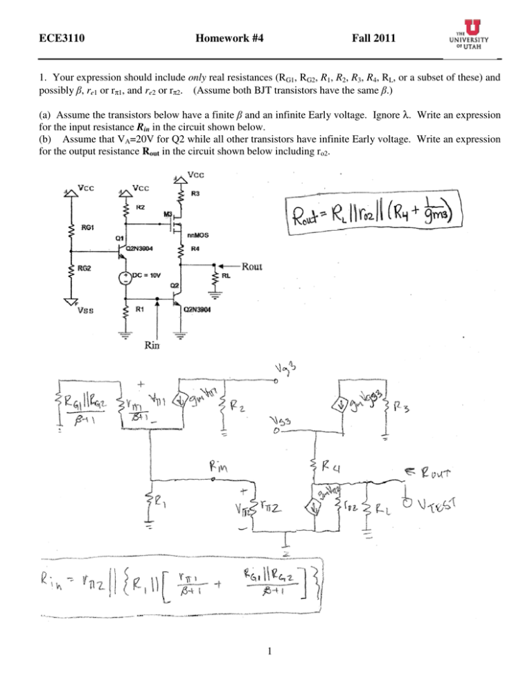
ECE3110 Homework #4 Fall 2011 1. Your expression should include only real resistances (RG1, RG2, R1, R2, R3, R4, RL, or a subset of these) and possibly β, re1 or rπ1, and re2 or rπ2. (Assume both BJT transistors have the same β.) (a) Assume the transistors below have a finite β and an infinite Early voltage. Ignore λ. Write an expression for the input resistance Rin in the circuit shown below. (b) Assume that VA=20V for Q2 while all other transistors have infinite Early voltage. Write an expression for the output resistance Rout in the circuit shown below including ro2. 1 ECE3110 Homework #4 Fall 2011 2. (a) Circle the answer that is the most appropriate: (i) Common-mode rejection ratio: 0.05 100 0.01 (ii) Common-mode gain: 0.05 100 0.01 (b) Answer True or False to the following questions: (i) Looking at the circuit on the right, if Re is increased, the gain increases. FALSE (ii) The input offset voltage for a BJT differential amplifier is directly related to a change in input signal. FALSE (iii) Input bias current in a MOS differential amplifier is due to the difference in (W/L) of the transistors. FALSE (iv) The input offset voltage for a MOS differential amplifier increases with an increase in Ibias. TRUE 3. An uncompleted circuit consisting of two differential pairs is shown below. We wish to create a biasing network so that the NMOS differential pair has a differential gain equal to 100V/V, and the pnp differential pair transistors each have a gm of 15.36mA/V. Assume that β is very large, kn’(W/L)=1.2mA/V2, |VBE| = 0.7 V, |VA|=40V, (threshold voltage) Vt=0.5V, and (thermal voltage) VT = 25 mV for this entire problem. Neglect the Early Effect for the BJT transistors. (a) State the required dc bias voltage (VGS) needed for the NMOS differential pair to work correctly.(See next page) (b) What value of I1 is required?(See next page) (c) What value of I2 is required? (d) Now, on the schematic below, draw a current mirror biasing network to provide the required dc currents. You may use no more than 3 nmos transistors, 5 pnp transistors, and one resistor of any value. Assume all transistors of the same type are identical in size. You may only use VDD= +5 V power supply. (Don’t worry about connecting anything to the inputs or outputs of the differential pairs; we’re only concerned with the biasing network in this problem. Assume that the MOSFET’s are biased to a saturation region. Don’t worry about the resistor values in the collector of the BJT.) 2 ECE3110 Homework #4 Fall 2011 3 ECE3110 Homework #4 Fall 2011 4. An active-loaded MOS differential amplifier is shown below. The transistors are specified as follows: (W/L)n=10, (W/L)p=20, kn’=2kp’=200µA/V2, |VA|=100V, VDD=10V, and |Vt|=0.7V. Design the circuit below so that Ad= 60V/V. (a) State the value needed for I and R. (b) Determine CMRR. (c) What is the voltage range for VCM. (minimum and maximum values for the input gates) 4 ECE3110 Homework #4 Fall 2011 5. Consider the basic bipolar differential circuit(shown to the right) in which the transistors have VDD=10V, β=100 and VA=100V, and RC=20kΩ. Find: (a) The value of RE. (b) the differential gain(Vo2-Vo1)/vid (b) the differential input resistance (c) the common-mode rejection ratio when the resistors in the collector are 2% accurate. 5 ECE3110 Homework #4 Fall 2011 CMRR = 2*(50e-6/25m)*REE/(0.02) where REE is the equivalent R of Widlar: REE=(1+gm*(RE||ro))*ro ro=VA/Ic=100/100e-6=1Meg REE= (1+(100e-6/25e-3)*((479*1x106)/(479+1x106)))*1Meg=2.92x106 CMRR=2*(50e-6/25e-3)*2.92x106/0.02=583,000 6 ECE3110 Homework #4 Fall 2011 Design the circuit below to achieve a DC bias of IE=1mA. Use β=100 and VA=50V for all transistors. Assume VBE=0.7V. 6. (a) State the value of IREF. (b) Derive an expression for Rin, Rout, and AM(midband gain) 7. (a) Select values for CE and CC to place the 2 break frequencies at 10Hz and 100Hz. (b) Calculate fH when Cπ=16pF, Cµ=0.3pF, and ignore rx. (Ignore the frequency effect due to the current source) 7 ECE3110 Homework #4 Fall 2011 8 ECE3110 Homework #4 Fall 2011 8. Use gm=1mA/V, Cgs=2pF, and Cgd=0.4pF. Find: (a) fL, (b) Am(midband gain), (c) fH. 9 ECE3110 Homework #4 Fall 2011 9. Assume all transistors are matched. The transistors are specified as follows: (W/L)n=10, (W/L)p=20, kn’=2kp’=200µA/V2, |VA|=100V, and |Vt|=0.7V. (a) Determine the overdrive voltage. (b) What is the allowable voltage range at the output (drain of Q2). 10 ECE3110 10. (a) (b) (c) (d) Homework #4 Fall 2011 Use β=100 and VA=50V for all transistors. Assume VBE=0.7V and VBC(on)=0.4V. Find Rin Rout1 Vo1/vin Approximate value of Vo2/vin 11
