WaferSense™ Auto Gapping System Theory of Operation
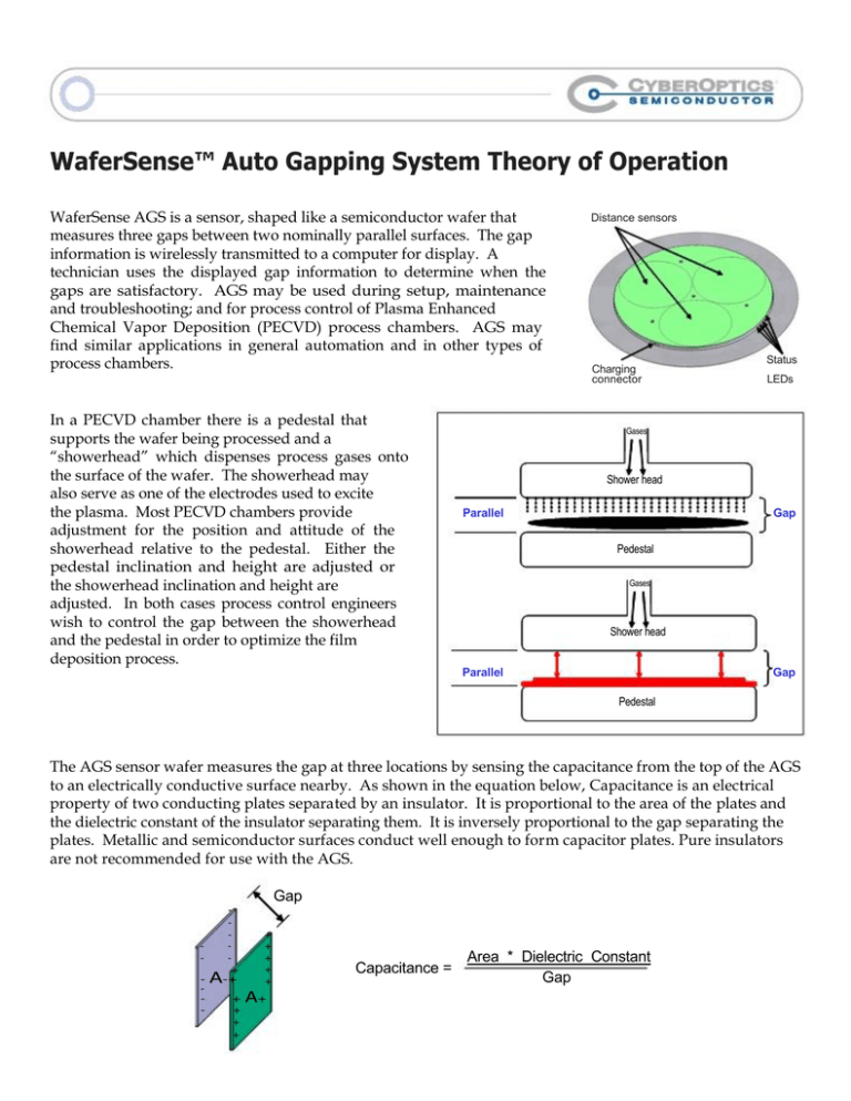
WaferSense AGS is a sensor, shaped like a semiconductor wafer that
measures three gaps between two nominally parallel surfaces. The gap
information is wirelessly transmitted to a computer for display. A
technician uses the displayed gap information to determine when the
gaps are satisfactory. AGS may be used during setup, maintenance
and troubleshooting; and for process control of Plasma Enhanced
Chemical Vapor Deposition (PECVD) process chambers. AGS may
find similar applications in general automation and in other types of
process chambers.
In a PECVD chamber there is a pedestal that
supports the wafer being processed and a
“showerhead” which dispenses process gases onto
the surface of the wafer. The showerhead may
also serve as one of the electrodes used to excite
the plasma. Most PECVD chambers provide
adjustment for the position and attitude of the
showerhead relative to the pedestal. Either the
pedestal inclination and height are adjusted or
the showerhead inclination and height are
adjusted. In both cases process control engineers
wish to control the gap between the showerhead
and the pedestal in order to optimize the film
deposition process.
Distance sensors
Charging
connector
Status
LEDs
Gases
Shower head
Parallel
Gap
Pedestal
Gases
Shower head
Parallel
Gap
Pedestal
The AGS sensor wafer measures the gap at three locations by sensing the capacitance from the top of the AGS
to an electrically conductive surface nearby. As shown in the equation below, Capacitance is an electrical
property of two conducting plates separated by an insulator. It is proportional to the area of the plates and
the dielectric constant of the insulator separating them. It is inversely proportional to the gap separating the
plates. Metallic and semiconductor surfaces conduct well enough to form capacitor plates. Pure insulators
are not recommended for use with the AGS.
+
- A-+
+
+
+
+
Gap
+
+
+
+
+
A+
Capacitance =
Area * Dielectric Constant
Gap
Finally, the gap may be calculated from the measured capacitance. AGS plate area is designed to optimize
measurement range and resolution. Measurement accuracy is a function of the gap. Accuracy is generally
better with smaller gaps. The following table shows how the worst case gap measurement accuracy
depends on the gap.
Accuracy (microns)
Accuracy as a function of Gap
80
60
40
20
0
10 11 12 13 14 15 16 17 18 19 20
Gap (mm)
Films which may develop on the showerhead do not affect the capacitance significantly because they are
thin relative to the total gap between the AGS and the showerhead. The effect of such films is smaller than
the sensor accuracy. In practice, showerhead flatness issues tend to be larger than showerhead surface
film issues.
Capacitance is a property of an area, not a single point; so warp and bow do not affect the measurement
significantly. The AGS is not designed to measure concavity, convexity, ripple and twist or other flatness
characteristics of either showerheads or pedestals. The measured gap is the composite gap over the
area of each distance sensor. It is representative of the distance over which the process gas flows to reach
the wafer.
Holes in the showerhead may affect gap measurement accuracy, but do not affect gap measurement
resolution or inclination accuracy significantly. Small aperture holes have a negligible affect on accuracy. Large
holes make the showerhead seem farther away than it truly is. In this case, technicians may place the AGS
into a chamber that is working well to determine its apparent gap. Thereafter, each chamber can be adjusted
to that set point.
The AGS converts raw capacitance data into gap information using an internal computer that references
sensor calibration data and sensor temperature data. Calibration is performed at the CyberOptics
Semiconductor factory using a computer controlled gap between two temperature controlled flat plates.
Annual sensor calibration is recommended to assure long term measurement accuracy.
The AGS is powered by a rechargeable battery with a 10 year shelf life. The battery is capable of storing at least
80% of its original power after 500 full discharge-recharge cycles. Storage and/or operation of the
AGS battery at temperatures higher than 80C will decrease the amount of power that the battery can hold. The
AGS battery temperature should never exceed 100C. The battery is not user serviceable. It is replaced during
the calibration service.
Wireless Communication: WaferSense AGS uses
WaferSense AGS
Vacuum
Robot
FOUP
Load port
EFEM or
Atmospheric
Front End
Process Tool
2.4 GHz RF (Bluetooth®) wireless communication
between the wafer and the link that is connected to a
PC. WaferSense AGS uses a Class 1 Bluetooth device,
rated for unimpeded communication up to 100
meters. Metal enclosures specific of a semiconductor
use environment do not inhibit this communication.
Link & Laptop: The link is a compact USB 1.1
compliant device that connects to a laptop to enable
wireless communication with the teaching wafer.
GapView™ Software Application: GapView
displays numerical and graphical gap information.
Each graphic is color-coded to make it easy to see
whether it is above, below or within the selected
target gap range.
Gap View can log time-stamped measurements to a
CSV (comma separated values) file for
documentation and/or analysis.
CSsupport@cyberoptics.com
For information about CyberOptics'
offices and global support network,
please visit www.cyberoptics.com.
www.cyberoptics.com
CSsupport@cyberoptics.com
Copyright © 2014, CyberOptics Corporation. All rights reserved. All tradenames are the registered property of their respective owners. 922-0126-01 Rev. B


