WHITE PAPER
Ultra-Low Noise Figure, High Gain Amplifier with High
Linearity
Introduction
Infrastructure receiver applications for cellular/3G, ISM, GPS,
WiMAX/4G, automotive applications, and satellite radio require
Low-Noise Amplifiers (LNAs) with very low Noise Figures (NF),
good input and output return loss, high linearity, low current, wide
band stability, and robust performance. These conflicting design
requirements are equally important, so they have to be achieved
simultaneously. These challenging requirements demand highest
available performance from the technology. To obtain an
optimized performance with minimum trade-offs, unique design
techniques and superior pHEMT process technology are used.
This White Paper describes different trade-offs, design options,
and implementation of a sub 1 dB low NF (~ 0.6 dB), high gain
(> 20 dB), and very high linearity (> +34 dBm) two-stage LNA.
The SKY65040-360LF LNA maintains a very low NF up to 2.5 GHz
and an excellent 3rd Order Output Intercept Point (OIP3). The
design is fabricated using Skyworks proprietary low-noise, high
linearity depletion-mode pHEMT process. It is an ideal building
block for base stations and satellite radios where NF and linearity
(IIP3) are very critical. Typical applications include GSM, PCS,
WCDMA, TD-SCDMA base stations, GPS and satellite radios.
LNA Topology and Technology
Design Requirements
LNA is designed specifically for WCDMA base station applications.
Therefore, the 3rd order intercept point (IP3) and 1 dB
compression point (P1dB) requirements for this LNA are also very
critical [1]. The usual technique of designing for low NF and
power gain, and later tuning the design for good linearity, may not
result in the optimum design trade-offs.
Output Return Loss (ORL) is given as the only parameter that has
a secondary importance and can be traded off for better IP3.
Design Architecture
Low noise operation of an amplifier requires the bias current to be
chosen around 15 to 25 percent of the drain source current (IDSS)
with the gate source voltage (VGS) = 0. However, high linearity
operation requires the bias current to be around 70 to 80 percent
of IDSS. The low NF and very high IP3 specifications dictate using
about 20 percent of IDSS for the first stage and the remaining
current used for the second stage to achieve a high IP3.
With a cascaded design, first and second stages can be biased at
different conditions. Individual voltage and current adjustment of
each stage provides extra flexibility needed for further
optimization. Gain and IP3 of the first or second stage can also be
adjusted independently with minimum effect on NF. Therefore, a
two stage LNA topology with cascaded common-source
amplifying stages seems to provide the most flexibility and,
therefore, optimum design trade offs.
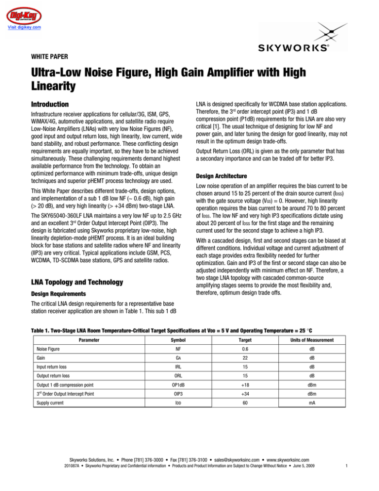
The critical LNA design requirements for a representative base
station receiver application are shown in Table 1. This sub 1 dB
Table 1. Two-Stage LNA Room Temperature-Critical Target Specifications at VDD = 5 V and Operating Temperature = 25 °C
Parameter
Symbol
Target
Units of Measurement
NF
0.6
dB
Gain
GA
22
dB
Input return loss
IRL
15
dB
Output return loss
ORL
15
dB
Output 1 dB compression point
OP1dB
+18
dBm
3rd Order Output Intercept Point
OIP3
+34
dBm
Supply current
IDD
60
mA
Noise Figure
Skyworks Solutions, Inc. • Phone [781] 376-3000 • Fax [781] 376-3100 • sales@skyworksinc.com • www.skyworksinc.com
201087A • Skyworks Proprietary and Confidential information • Products and Product Information are Subject to Change Without Notice • June 5, 2009
1
WHITE PAPER • LOW NF, HIGH LINEARITY LOW NOISE AMPLIFIER
Table 2. Initial System Budget Calculations for NF and OIP3
Stage Data
Noise Figure
Stage 1
Stage 2
Units of Measurement
0.5
2.0
dB
Gain
13
9
dB
3rd Order Output Intercept Point
+30
+36
dBm
Supply current
22
40
mA
Stage 1
Stage 2
Units of Measurement
Noise Figure
System
0.6
–
dB
Gain
22
–
dB
rd
+34.2
–
dBm
3 Order Output Intercept Point
100
VGS = 0
m7:
VDS = 5.0 V
IDS = 4 mA
VGS = –0.8 V
IDS (mA)
80
VGS = –0.2 V
60
VGS = –0.4 V
40
20
VGS = –0.6 V
m7
VGS = –0.8 V
0
0
0.714
1.429
2.143
2.857
3.571
4.286
5.000
VDS (V)
Figure 1. IV Curves of 300 μm Device
The IP3 can be further improved by presenting different
impedance terminations to the device [2]. When more current is
available, the second stage drain current can always be increased
to improve IP3 and P1dB with a minimal impact on other
performance parameters.
The initial cascaded analysis of a two-stage LNA is shown in
Table 2. A good system budget analysis helps optimize the design
and eliminates early mistakes. Higher gain for the first stage
reduces the effect of the second stage in the overall NF and
provides most of the necessary gain.
Process Technology and Biasing
This design uses Skyworks depletion mode, Low Noise Field
Effect Transistor (LNFET) with a Thin Film Resistor (TFR) process.
The LNFET/TFR 0.5 μm gate length process is specifically
designed for superior low noise performance in high linearity
applications. Accurate, proprietary models enable effective circuit
design simulations.
To understand various trade-offs in biasing considerations, a
300 μm size device is used as a test vehicle for the first stage.
Simulations were run using the Agilent ADS simulation tool. The IV
curves of a 300 μm device are shown in Figure 1.
The graph in Figure 2 shows the maximum available gain versus
drain current and voltages. The gain drops rapidly as the drain
current goes below 20 mA (drain source voltage, VDS= ~ –0.6 V,
20 percent of IDSS). These plots also show that the gain stays
about constant from VDS = 2 to 5 V. Figure 3 shows minimum NF
versus VDS with varying VGS.
Due to the nature of depletion mode technology, biasing the FET
for optimum operation requires negative gate-to-source voltage.
The current at the device saturating region is given by the
following equation:
⎛
V
I DS = I DSS ⎜⎜ 1 − GS
VP
⎝
⎞
⎟
⎟
⎠
2
Where VGS and VP (pinch-off voltage) values are both negative.
A drain current of 20 mA corresponds to about –0.42 V of VGS
voltage. A self biasing network that eliminates a negative supply
at the gate terminal is designed for optimum operation as shown
in Figure 4. With this biasing technique, a resistor at the source
(RS) is used to set the positive source DC voltage and drain
current. A large value bypass capacitor is needed to bypass RS.
Skyworks Solutions, Inc. • Phone [781] 376-3000 • Fax [781] 376-3100 • sales@skyworksinc.com • www.skyworksinc.com
2
June 5, 2009 • Skyworks Proprietary and Confidential information • Products and Product Information are Subject to Change Without Notice • 201087A
VGS = 0
VGS = –0.2 V
VGS = –0.4 V
VGS = –0.6 V
+25
0.6
Noise Figure, Min. (dB)
Maximum Available Gain (dB)
WHITE PAPER • LOW NF, HIGH LINEARITY LOW NOISE AMPLIFIER
VGS = –0.8 V
+15
VGS = –1.0 V
+5
VGS = 0
0.5
VGS = –0.2 V
m10:
VDS = 5.000 V
NFmin[0] = 190 dB
VGS = –0.6 V
0.4
0.3
VGS = –0.4 V
m10
0.2
VGS = –0.6 V
VGS = –0.8 V
–5
0
1
2
3
4
0.1
5
0
1
2
3
4
5
VDS (V)
VDS (V)
Figure 2. Maximum Available Gain vs VGS (Current) at Varying VDS
for a 300 μm Device
Figure 3. Minimum NF vs VGS and VDS for a 300 μm Device
+
–
VDC
SRC2
VDC = VHIGH
L1
1 μH
C2
1 μF
VLOAD
C12
1 μF
+
Z = 50 Ω
+
Z = 50 Ω
S
fetLN2_1
L7
1 mH
–
–
L3
1.2 nH
R2
21 Ω
C8
1 μF
Figure 4. Amplifier Schematic Showing the FET Self-Bias Circuit
A simple method of a shunt inductor (or a very large value of
shunt resistor) at the gate can be used for gate DC biasing. This
inductor can also be used as part of the input matching network.
A source resistor value of 21 Ω allows a VGS voltage drop of
–0.42 V between the gate and source terminals as shown in
Figure 4.
Figure 5 shows available gain and noise circles on a Smith chart
for a single stage design. The graph shows that gain starts to
trade off with the NF if higher gain is desired from a single stage.
Also, in a two-stage design as the gain of the first stage
increases, IP3 and P1dB start to degrade due to earlier saturation
of the second stage. Therefore, optimum trade-off between the
gain, NF, and P1dB should be selected for the first stage. The
system budget calculation shown in Table 2 allocates about 13 dB
of gain for the first stage and 9 dB of gain for the second stage
with a 2 dB gain margin allocated for the other circuit losses.
However, the second stage is mainly designed for P1dB and IP3
performance. Higher current provides higher OIP3 but the
maximum total current specification of 60 mA forces allocation of
about 45 mA to the second stage.
Design for Optimum NF and Input Match
Two of the design constraints, NF and input return loss, are the
main factors used to determine the first stage design. Based on
the design considerations discussed earlier, the total device
periphery of 300 μm is chosen for the first stage. This was mainly
done to provide broadband gain performance with low current
Skyworks Solutions, Inc. • Phone [781] 376-3000 • Fax [781] 376-3100 • sales@skyworksinc.com • www.skyworksinc.com
201087A • Skyworks Proprietary and Confidential information • Products and Product Information are Subject to Change Without Notice • June 5, 2009
3
WHITE PAPER • LOW NF, HIGH LINEARITY LOW NOISE AMPLIFIER
operation at the same time. The IDSS for this device is around
90 mA.
The device is biased at 20 mA current for optimum NF and gain
trade off. The target for total NF shown in Table 2 is 0.6 dB.
System analysis shows that the NF has to be below 0.5 dB for the
first stage. The bare FET device provides a minimum NF of about
0.3 dB. This leaves about 0.2 dB of NF degradation for all other
factors.
About 0.05 dB of loss can be allocated to the resistive losses due
to the bias circuitry at 2 GHz and source inductor resistive losses.
This allows for about 0.15 dB of resistive loss for the input match,
assuming that the input is matched for the optimum NF
impedance.
To meet 0.15 dB of input match resistive loss at 2 GHz, Agilent
ADS simulations show that quality factors > 60 for inductors, and
> 200 for capacitors are needed.
The inductive degeneration technique is used for simultaneously
optimizing NF and input match.
Design for Linearity (IP3) and P1dB
As mentioned earlier, P1dB and IP3 determine the second stage
design. The measured device data available was at an input
power (PIN) = –18 dBm. However, the system gain allocations
show that a PIN ~ –5 dBm is present at the input of the second
stage device. Therefore, simulation models are used to estimate
OIP3 at PIN = –5 dBm.
The OIP3 and P1dB simulations were performed using 50 Ω input
and output impedance conditions at 2 GHz. Figure 6 shows P1dB
and OIP3 contours. Simulations show around +18 dBm P1dB and
+33 dBm OIP3 are achievable. Since the OIP3 requirement is
higher than what 50 Ω source and load conditions provide,
source and load matching needs to be done to improve OIP3.
Input and output terminations in band and out of band directly
affect the linearity performance of the amplifier. The input and
output terminations of the amplifier can be swept directly through
source and load pull techniques. The Agilent ADS large signal
source and load pull setup are shown in Figure 7.
Figure 5. Available Gain and Noise Circles
Skyworks Solutions, Inc. • Phone [781] 376-3000 • Fax [781] 376-3100 • sales@skyworksinc.com • www.skyworksinc.com
4
June 5, 2009 • Skyworks Proprietary and Confidential information • Products and Product Information are Subject to Change Without Notice • 201087A
WHITE PAPER • LOW NF, HIGH LINEARITY LOW NOISE AMPLIFIER
m1:
indep(m1) = 1
Pdel_contours_p = 0.791/93.343
level = 2.342131, number = 1
impedance = 10.869 + j45.971
m4:
indep(m4) = 11
OIP3_low_contours_p = 0.135/–40.281
level = 38.309698, number = 1
impedance = 60.460 – j10.776
OIP3_low_contours_p
Pdel_contours_p
m1
m4
Indep(Pdel_contours_p) (0.000 to 35.000)
indep(OIP3_low_contours_p) (0.000 to 45.000)
Figure 6. OIP3 and Delivered Power Contours
Two-tone, load pull simulation: output power, PAE,
third and fifth order intermodulation distortion levels
found at each fundamental load impedance.
Specify desired fundamental load tuner coverage:
s11_rho is the radius of the circle of simulated reflection coefficients. However, the radius of
the circle is reduced if it would otherwise go outside the Smith Chart. To override this and
allow reflection coefficients outside the Smith Chart, edit the Sweep Equations VAR block and
set maximum rho = maximum available gain (s11_rho).
s11_center is the center of the circle of simulated reflection coefficients.
pts is the total number of reflection coefficients simulated.
Z0 is the system reference impedance.
+
–
+
–
VAR
Sweep Equations
s11_rho = 0.9
s11_center = 0 + j*0.0
pts = 100
Z0 = 50 Ω
+
–
Parameter Sweep
Sweep 1
Set these values:
VAR
STIMULUS
Available source power (Pavs) = –6 dBm
RF freq = 2 GHz
freq spacing = 10 MHz
5th order max IMD
Vhigh = 5 V
Harmonic Balance
HB1
MaxOrder = Max_IMD_order
Freq[1] = RF freq – fspacing/2
Freq[2] = RF freq + fspacing/w2
Order[1] = 7
Order[2] = 7
UseKrylov = No
Figure 7. Agilent ADS Large Signal Source and Load Pull Test Setup for a Common Source pHEMT Amplifier
Skyworks Solutions, Inc. • Phone [781] 376-3000 • Fax [781] 376-3100 • sales@skyworksinc.com • www.skyworksinc.com
201087A • Skyworks Proprietary and Confidential information • Products and Product Information are Subject to Change Without Notice • June 5, 2009
5
WHITE PAPER • LOW NF, HIGH LINEARITY LOW NOISE AMPLIFIER
The inter-stage matching network determines the IP3 input
source termination for the second stage. To determine the
optimum impedance for best OIP3, a source and load pull is
performed independently. Impedance points are shown in
Figure 6.
Load pull results show that with a 50 Ω source impedance, the
maximum OIP3 that can be achieved is +35.7 dBm. Source pull
results with a 50 Ω load impedance show that a maximum OIP3
of +39 dBm can be achieved. Based on this data, a source
impedance point of ZS = 20 + j60 Ω that provides an OIP3 of
about +37 dBm OIP3 is chosen. After the source is matched, load
pull is performed again. Figures 8 and 9 show P1dB and OIP3
results, respectively, after the source is matched.
Simulations show that a maximum OIP3 of around +43 dBm can
be achieved after source and load pull when both are matched for
best OIP3. When this is designed as the second stage of a
cascaded amplifier, the input match serves as a matching circuit
between the first and the second stage. Final load pull simulation
and matching should be done after connecting the two stages
together.
Design For Stability
Stability is one of the most important requirements to consider for
an LNA. Typical specifications dictate unconditionally stable
operation up to 18 GHz. Each stage must be designed for
unconditionally stable operation as well as the total two stage
design that includes all the external components and biasing over
all conditions.
and meet these requirements, multiple stability design techniques
have been used. To solve stability problems at low to higher
operating frequencies, some value of a source inductor is
generally used.
A source degeneration inductor is used for input; a NF match can
be used for this purpose as well. One technique that is commonly
used is to have a series-parallel LR network. This network
behaves like a low impedance at low frequencies and a high
impedance at higher frequencies. Another technique that is
commonly used is a shunt-series CR network connected from
drain to ground. This network behaves like a shunt resistor at high
frequencies and high impedance at low frequencies. A shunt
resistor connected to ground helps to stabilize the device.
Another method that is used to improve stability is the shunt
feedback between the output and the input of the device.
However, this method degrades the NF. Therefore, it is not used
in the first stage design but is used in the second stage design.
This feedback also helps the IP3, return loss, and gain
adjustment.
Figures 10 and 11 show stability results before and after these
stability techniques are used, respectively. Figure 10 shows that
the design is stable only within a small frequency band. After
using the stabilizing circuits, the design becomes unconditionally
stable from 0.05 to 18 GHz as shown in Figure 11. Stabilizing
circuits are integrated into the two-stage cascaded LNA. Final
simulation and measurement results are presented in the
following section.
A very low noise device with high gain usually becomes highly
unstable in most of the frequency range. To stabilize the device
+38
m14
m15:
Avail source power = –6 dBm
OIP3, low = +37.599
m15
+36
+20
+15
m14:
Avail source power = +10 dBm
Delivered power = +19.464
+10
+5
0
–10
OIP3, Low (dBm)
Delivered Power (dBm)
+25
+34
+32
+30
+28
–8
–6
–4
–2
0
+2
+4 +6
+8
Available Source Power (dBm)
Figure 8. P1dB After Source is Matched
+10 +12
+26
–10
–8
–6
–4
–2
0
+2
+4
+6
Available Source Power (dBm)
Figure 9. OIP3 After Source is Matched
Skyworks Solutions, Inc. • Phone [781] 376-3000 • Fax [781] 376-3100 • sales@skyworksinc.com • www.skyworksinc.com
6
June 5, 2009 • Skyworks Proprietary and Confidential information • Products and Product Information are Subject to Change Without Notice • 201087A
+8
+10
+12
WHITE PAPER • LOW NF, HIGH LINEARITY LOW NOISE AMPLIFIER
3
3
2
2
Stability
Stability
m7:
Freq = 1.1 GHz
K = 0.912
m7
m7:
Freq = 1.1 GHz
K = 1.126
1
1
m7
m8:
Freq = 8.1 GHz
b = 0.074
m8
m8:
Freq = 8.1 GHz
b = 0.661
m8
0
0
0
2
4
6
8
10
12
14
16
18
0
2
4
6
8
10
12
14
16
18
Frequency (GHz)
Frequency (GHz)
Figure 11. After Stability Fixing Circuit Added
Figure 10. Before Stability Fixing Circuit Added
Figure 12. Bare Test Board
Test Board Layout and Grounding
A good test board design is important to achieve the expected
performance. Special attention must be given to minimize
unwanted parasitics and to ensure proper grounding. Grounding is
particularly important to simultaneously ensure high gain and
unconditional stability.
As can be seen in Figure 12, a grounded Coplanar Waveguide
(CPW) transmission line was used for component tuning flexibility
and provides signal isolation due to its top ground metal. The test
board was realized on an FR4 VT-47 (0.254 mm thick) for its
lower loss, cost, and reasonably low dielectric constant.
An automated board assembly requires minimum spacing rules to
be followed. Selecting a very high dielectric constant material
may make the circuit very small but it can also turn design rule
spacings into undesired phase shifts. The line width and spacing
to the ground plane were selected to fit shunt 0402 sized surface
mount components while maintaining a uniform 50 Ω line even
when shunt components are not populated.
Vias are used on each side of CPW lines to reach the bottom
common ground plane. Vias are inductive and their inductance is
a factor of their aspect ratio. Although vias having a bigger
diameter for a fixed length are less inductive and therefore
preferred, their size may prevent placement in required locations.
As frequency increases, vias become increasingly inductive. This
may result in an RF feedback path through the top ground metal,
leading to instabilities. For that reason, the top ground plane is
intentionally broken in various sections to open any potential RF
current feedback loops. The remaining metal islands are
grounded to avoid creating unwanted resonators. More vias are
used along the metal edges for improved high frequency
performance.
Vias should also be placed as close as possible to board
components to minimize the electrical length to the ground
Skyworks Solutions, Inc. • Phone [781] 376-3000 • Fax [781] 376-3100 • sales@skyworksinc.com • www.skyworksinc.com
201087A • Skyworks Proprietary and Confidential information • Products and Product Information are Subject to Change Without Notice • June 5, 2009
7
WHITE PAPER • LOW NF, HIGH LINEARITY LOW NOISE AMPLIFIER
components C15 and C16 are typically populated with a capacitor
and a resistor, respectively.
reference, which includes the vias’ length. Although electrical
lengths may be very small in the band of operation, they can be a
source of important phase shifts at high frequencies. The most
ground-sensitive regions to achieve good performance of the LNA
are the input matching circuit and the RF decoupling regions of
the drain and source terminals of each stage. Both of these
important areas are addressed in the Evaluation Board design by
adding vias to minimize parasitic inductance.
The input and noise matching network is composed of
components C1, L1, and L2. As any source of loss at the input of
an LNA directly contributes to its NF, the components used at the
input must have a reasonably high quality factor. Output match is
achieved by components C10, L5, and L6.
Out of band oscillations are addressed by additional capacitors C8
and C9 to decouple lower frequencies traveling through the choke
inductors at both stages. Capacitors C2, C3, and C13 decouple
the highest frequencies up to 18 GHz. The placement of these
capacitors is critical to avoid instability at these frequencies.
Resistors R3 and R4 also contribute to stability as they present a
higher resistance to RF from output to input of the device.
Component Selection Considerations
Component selection is affected by various factors such as
component parasitics, the component location in the circuit, the
frequency range of operation, and the intended purpose for the
component.
Figure 13 shows the test board circuit schematic. A feedback
circuit can be used if gain adjustment is needed. In that case,
VDD
C10
C7
R3
R5
C9
C6
L5
L4
1
C2
L1
2
RF Input
C1
C3
3
8
VDD1
N/C
C11
7
RFIN
BIAS1
RFOUT/VDD2
SKY65040
×
R1
L5
5
BIAS2
FEEDBACK
R4
R2
L6
RF Output
6
N/C
L2
4
×
C8
C5
C4
S1501
Figure 13. Evaluation Board Schematic
Skyworks Solutions, Inc. • Phone [781] 376-3000 • Fax [781] 376-3100 • sales@skyworksinc.com • www.skyworksinc.com
8
June 5, 2009 • Skyworks Proprietary and Confidential information • Products and Product Information are Subject to Change Without Notice • 201087A
WHITE PAPER • LOW NF, HIGH LINEARITY LOW NOISE AMPLIFIER
Measured vs Simulated Results
A manufactured amplifier was tested on the test board at a supply
voltage (VDD) of 5 V. This voltage sets a bias point at the first stage
as VDS = 2.4 V at a drain voltage (ID) = 23 mA, and a bias point at
the second stage as VDS = 4.2 V at ID = 46 mA.
Figure 14 shows measured and simulated NFs in a bandwidth of
1.92 to 1.98 GHz. The loss of the input transmission line was
measured as 0.1 dB in this band. The NF is measured as 0.65 dB
at 1.95 GHz after de-embedding the input transmission line loss.
Figure 15 shows simulated and measured two-stage amplifier
gain as functions of frequency. The gain is 24.8 dB at 1.95 GHz.
The inset in Figure 15 below is a narrow-band view of the gain
within the frequency band.
Figures 16 and 17 show simulated and measured input return
loss and output return loss, respectively. Both input and output
return loss measure greater than 20 dB in the passband.
Figure 18 shows measured OIP3 within the band. The input power
of –18 dBm per tone was applied at two fundamental frequencies
of 1947.5 and 1952.5 MHz.
Figure 19 shows input power at the 1 dB input compression point
(IP1dB), measured at –7.2 dBm. The output power at the 1 dB
output compression point (OP1dB) is measured at +17.6 dBm.
Conclusion
Many performance aspects must be considered in the design of
LNAs. Next generation LNAs require new technologies and design
techniques to meet the increasing demands of the market. An
optimized design with proprietary pHEMT technology discussed in
this White Paper will be required to meet the challenging
performance requirements of new products while keeping the
cost low and maintaining small size.
0.6
2.5
2.4
2.3
2.2
2.1
–40
1.96
1.98
–80
2.00
0
2
4
6
4
6
8
10
12
18
14
16
Frequency (GHz)
Figure 16. Simulated and Measured Input Return Losses
18
–20
16
18
0
–10
–20
2.5
2.4
2.3
2.2
2.1
2.0
1.9
–30
1.8
Frequency (GHz)
–30
2
16
Simulated
Measured
–10
Output Return Loss (dB)
2.5
2.4
2.3
2.2
2.1
2.0
1.9
1.8
1.7
1.6
–20
1.5
Input Return Loss (dB)
–10
–30
14
0
1.5
Output Return Loss (dB)
0
Simulated
Measured
12
Figure 15. Simulated and Measured Gain
0
–20
10
Frequency (GHz)
Figure 14. Simulated and Measured Noise Figure
–10
8
1.7
1.94
1.6
1.92
Frequency (GHz)
Input Return Loss (dB)
2.0
Frequency (GHz)
Simulated
Measured
0.5
1.90
0
1.9
1.5
0
28
25
22
19
16
13
1.8
0.7
1.7
Gain (dB)
30
1.6
Simulated
Measured
Gain (dB)
Noise Figure (dB)
0.8
Frequency (GHz)
–30
0
2
4
6
8
10
12
14
Frequency (GHz)
Figure 17. Simulated and Measured Output Return Losses
Skyworks Solutions, Inc. • Phone [781] 376-3000 • Fax [781] 376-3100 • sales@skyworksinc.com • www.skyworksinc.com
201087A • Skyworks Proprietary and Confidential information • Products and Product Information are Subject to Change Without Notice • June 5, 2009
9
WHITE PAPER • LOW NF, HIGH LINEARITY LOW NOISE AMPLIFIER
26
+39
25
+38
+37
24
Gain (dB)
OIP3 (dBm)
+36
+35
+34
+33
23
22
+32
+31
21
+30
+29
1920
1930
1940
1950
1960
1970
1980
Frequency (MHz)
Figure 18. Measured Output 3rd Order Intercept Point
20
–20 –19 –18 –17 –16 –15 –14 –13 –12 –11 –10
–9
–8
–7
–6
Input Power (dBm)
Figure 19. Measured Input Power at 1 dB Compression Point
References
1. Chen, Seng-Woon, Linearity Requirements for Digital Wireless
Communications, Gallium Arsenside Integrated Circuit (GaAs IC)
Symposium, 1997, Technical Digest, 19th Annual, pp. 29-32,
October 1997.
2. Maas, Stephen A., Nonlinear Microwave Circuits, IEEE Press,
pp. 349-351.
Copyright © 2009 Skyworks Solutions, Inc. All Rights Reserved.
Information in this document is provided in connection with Skyworks Solutions, Inc. (“Skyworks”) products or services. These materials, including the information contained herein, are provided by
Skyworks as a service to its customers and may be used for informational purposes only by the customer. Skyworks assumes no responsibility for errors or omissions in these materials or the
information contained herein. Skyworks may change its documentation, products, services, specifications or product descriptions at any time, without notice. Skyworks makes no commitment to
update the materials or information and shall have no responsibility whatsoever for conflicts, incompatibilities, or other difficulties arising from any future changes.
No license, whether express, implied, by estoppel or otherwise, is granted to any intellectual property rights by this document. Skyworks assumes no liability for any materials, products or
information provided hereunder, including the sale, distribution, reproduction or use of Skyworks products, information or materials, except as may be provided in Skyworks Terms and Conditions
of Sale.
THE MATERIALS, PRODUCTS AND INFORMATION ARE PROVIDED “AS IS” WITHOUT WARRANTY OF ANY KIND, WHETHER EXPRESS, IMPLIED, STATUTORY, OR OTHERWISE, INCLUDING FITNESS FOR A
PARTICULAR PURPOSE OR USE, MERCHANTABILITY, PERFORMANCE, QUALITY OR NON-INFRINGEMENT OF ANY INTELLECTUAL PROPERTY RIGHT; ALL SUCH WARRANTIES ARE HEREBY EXPRESSLY
DISCLAIMED. SKYWORKS DOES NOT WARRANT THE ACCURACY OR COMPLETENESS OF THE INFORMATION, TEXT, GRAPHICS OR OTHER ITEMS CONTAINED WITHIN THESE MATERIALS. SKYWORKS
SHALL NOT BE LIABLE FOR ANY DAMAGES, INCLUDING BUT NOT LIMITED TO ANY SPECIAL, INDIRECT, INCIDENTAL, STATUTORY, OR CONSEQUENTIAL DAMAGES, INCLUDING WITHOUT LIMITATION,
LOST REVENUES OR LOST PROFITS THAT MAY RESULT FROM THE USE OF THE MATERIALS OR INFORMATION, WHETHER OR NOT THE RECIPIENT OF MATERIALS HAS BEEN ADVISED OF THE
POSSIBILITY OF SUCH DAMAGE.
Skyworks products are not intended for use in medical, lifesaving or life-sustaining applications, or other equipment in which the failure of the Skyworks products could lead to personal injury,
death, physical or environmental damage. Skyworks customers using or selling Skyworks products for use in such applications do so at their own risk and agree to fully indemnify Skyworks for any
damages resulting from such improper use or sale.
Customers are responsible for their products and applications using Skyworks products, which may deviate from published specifications as a result of design defects, errors, or operation of
products outside of published parameters or design specifications. Customers should include design and operating safeguards to minimize these and other risks. Skyworks assumes no liability for
applications assistance, customer product design, or damage to any equipment resulting from the use of Skyworks products outside of stated published specifications or parameters.
Skyworks, the Skyworks symbol, and “Breakthrough Simplicity” are trademarks or registered trademarks of Skyworks Solutions, Inc., in the United States and other countries. Third-party brands
and names are for identification purposes only, and are the property of their respective owners. Additional information, including relevant terms and conditions, posted at www.skyworksinc.com,
are incorporated by reference.
Skyworks Solutions, Inc. • Phone [781] 376-3000 • Fax [781] 376-3100 • sales@skyworksinc.com • www.skyworksinc.com
10
June 5, 2009 • Skyworks Proprietary and Confidential information • Products and Product Information are Subject to Change Without Notice • 201087A
