Application Note 1819
A 700W Broadband Amplifier Using
VRF2944
Introduction
This article describes a robust 700W 1.5-52 MHz broadband linear amplifier using the new
Microsemi VRF2944 power MOSFETs. The VRF2944 represents the latest in high power
VDMOSFET devices. With a minimum BVDSS of 170V, it will operate from a 65V supply allowing
the devices’ optimum output power to be obtained with a simple 4:1 broadband transformer. In this
circuit configuration, the VRF2944s are capable of providing 700W of continuous output power with
enough design headroom to survive the momentary impedance transients that occur in typical
operation. Features and requirements for all of the major components of the design are identified,
with sourcing information. A printed circuit board layout is provided.
Topology
The basic broadband transformer-coupled push-pull circuit topology has remained unchanged for
almost 70 years. The only changes over that time being the transformer construction, their ratios,
and supply voltage, as determined by the ever-increasing capabilities of active devices. Push-pull
operation offers several advantages over any single-ended design. First and foremost, it provides
twice the output, without using a separate combiner. Its inherent circuit balance suppresses the
even harmonics which then reduces the complexity of output lowpass filters needed for regulatory
compliance. A single-ended broadband circuit requires a very strong supply bypass capacitor at the
cold end of the output transformer, but in the push-pull circuit the supply voltage is applied at an
RF-neutral point. This greatly simplifies the design and lowers the stress on the bypass capacitors.
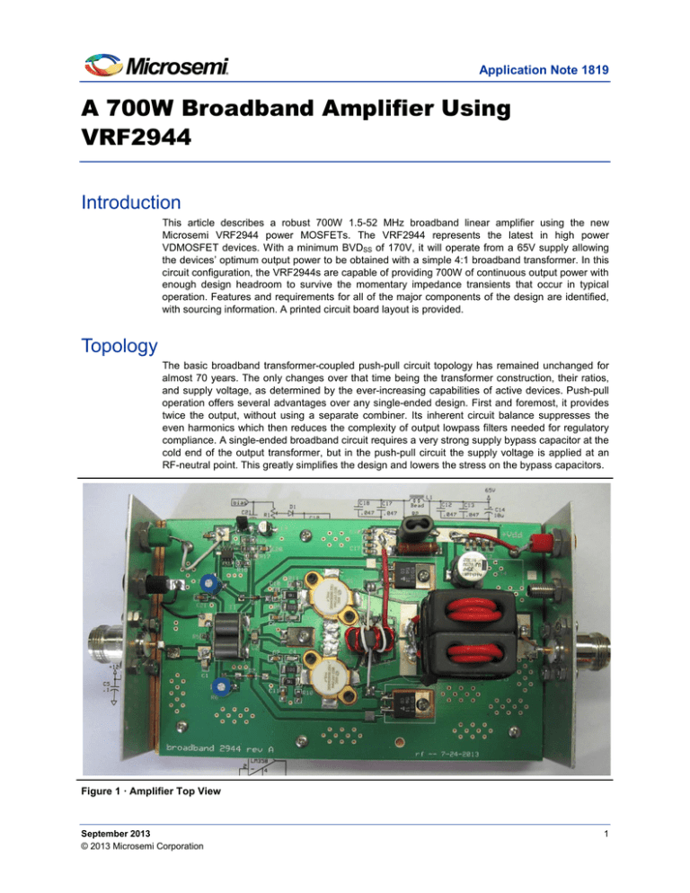
Figure 1 · Amplifier Top View
September 2013
© 2013 Microsemi Corporation
1
A 700W Broadband Amplifier Using VRF2944
Optimization
The relationship between the power supply voltage, drain-to-drain load impedance and output
power is expressed as
𝑃𝑜 =
2
2𝑉𝑑𝑑
𝑅𝐿
The rated output power of the VRF2944 is 400W. To add a little design headroom, especially for
when air-cooling is used, this will be reduced to 350W or 700W for the pair. The simplest and most
efficient broadband output transformers have an impedance ratio of 4:1. With a 50 Ω load, the
drain-to-drain load as seen through the transformer is 12.5 Ω. Rearranging the formula and solving
for Vdd gives 66V for this case.
𝑉𝑑𝑑 = �
𝑃𝑜 𝑅𝐿
2
The breakdown voltage of the VRF2944 is 170V minimum at DC. At RF, the actual breakdown
1
voltage is typically 25 to 30% higher than its DC value. The peak drain voltage under normal class
2
AB operation is typically two times the DC supply. So even operating the VRF2944 at 70V does
not violate the manufacturer’s specifications, and there is plenty of BV headroom left to cover any
transient or load mismatch events.
What we have established above is the notion of adjusting the supply voltage to make optimum use
of the device capability while using an easily-realized load impedance. This is the key to high power
broadband operation. For optimized operation at a single frequency, the designer is free to use
tuned matching networks. This is especially useful in the case of pulsed operation where the device
may be used for ten or even twenty times its nominal CW power but at a reduced duty cycle. The
maximum pulsed operation for MOSFETs is determined by either the pulsed drain current limit of
4x IDmax or the value of RDS(on).
A complete parts listing appears
at the end of this article.
Figure 2 · VRF2944 Broadband Amplifier
2
Transformers
Transformers
The input transformer T1 is a “bead and tube” type with 3:1 turns ratio. The secondary is brass
tubing fitted inside the two ferrite beads. The tubes are held in place by 32 mil circuit board end
caps that also serve to terminate and secure the transformer to the main circuit board. The three
turn primary is wound inside the tubing which reduces leakage flux and improves coupling, both
add to the bandwidth of the transformer. The center tap of the secondary is not grounded directly
which allows any difference current to be dissipated in R5. This usually improves balance as
3
observed by even harmonic suppression. The transformer is available premade. The leakage
inductance compensation is by accomplished by C2. It is optimized at 30 MHz for best input match.
T2 is a multi-function device. The seven turn bifilar #18 windings are the DC feed choke. The total
series impedance must be at least 100 Ω at the lowest frequency of operation. Because the DC
current flows in opposite directions in each wire, the net current is zero so the core does not
saturate. The third winding, 3t of #24 PTFE, is used to apply negative feedback to the gates. This is
a simple and reliable feedback method which also eliminates the need for a blocking capacitor.
4,5
The output transformer, T3, is both a 4:1 coaxial transformer and balun. It has two independent
coax lines that are loaded by ferrite cores. The ferrite loading on them makes their end-to-end or
common-mode impedance greater than 200 Ω at the lowest frequency of operation while keeping
the total coax length less than an eighth wave at the highest operating frequency. On the low
impedance input side at the drains, the two coaxes are connected in parallel. They are connected
in series on the output end which doubles the voltage and increases the impedance by a factor of
four. The coax Zo impedance required to do this is 25 Ω, the geometric mean between the input
and output impedances. The dissipation at 700W in most small coax, even PTFE types, becomes
an issue. 2.75mm diameter cable is best for high duty cycle applications. Small quantities can be
6
obtained readily. For a one-time build, paralleled pairs of RG-188 can be used. For commercial
7,8
applications, 2.75mm 25 Ω PTFE coax is readily available.
Any broadband amplifier has variations in gain, efficiency, saturated output power, and input VSWR
over its frequency range. The devices have an inherent gain slope. This is compensated by
resistive swamping the input circuit to provide a more constant input impedance. R3, 4, 7 and 9
plus C3 and 4 provide T1 with a reasonable load while increasing the drive towards the high
frequency end. Negative feedback, provided via R8 and R12 from the link on T2, works to suppress
the gain at the lower frequency end and further stabilizes the input impedance. The circuit layout of
the feedback link, rather long and circuitous, introduces inductance in the path which reduces the
amount of negative feedback towards the top end of the frequency range.
The output power and efficiency are determined by the effective load, 12.5 Ω in our case. However,
the devices’ output capacitance, COSS, introduces a parasitic shunt element across the drains. This
has the effect of reducing the effective source impedance with increasing frequency. It degrades
both the gain and efficiency. For single frequency operation, its effects can be removed by
resonating the COSS with a shunt inductor, sometimes incorporated into T2. A compensating
capacitor across the T3 input to can be used to provide a better single frequency match at the top
end. It must be a low loss type because of the very high RF currents involved. It is not used in this
amplifier.
As the bandwidth increases, transformer design becomes a most critical factor. Selection of the
ferrite and compensating for transformer leakage reactance are important. The ferrite must exhibit
low loss at the high end yet have enough permeability, μi, to provide the minimum necessary
impedance at the low frequency end. The losses are not insignificant and the output transformer
will run hot. The ferrite must have a Curie temperature > 200°C. Since T3 is both a transformer and
a balun, it must provide sufficient common mode impedance to isolate the grounded output terminal
from the drains. If not, the even harmonic suppression will suffer, hence the 200 Ω minimum Z at
the low frequency end.
3
A 700W Broadband Amplifier Using VRF2944
Thermals
No amplifier system is complete without its cooling system. If we assume that the devices will
operate at 50% efficiency, the RF output power will equal the DC power dissipated in the heatsink.
At peak power this amplifier will dissipate at least 750W, under severe load mismatch conditions
the dissipation can be two or three times that. The heatsink must have sufficient thermal mass to
absorb the transient heat load until other circuit protections can react. It should have a combination
of a copper heat spreading plate that is then attached to a high-density finned aluminum heat
dissipater or water-cooled cold plate. For air cooling, a forced air volume of at least 100CFM must
be available under conditions of high dissipation. To minimize noise, the fan can be speedcontrolled based on the heat sink temperature.
The MOSFET die temperature is limited to 200°C maximum. The device junctions have a very
small thermal mass so the die temperature can rise very quickly – far faster than a sink-mounted
thermal sensor can react. These devices have a thermal time constant of less than one second
while the heat sink’s time constant is measured in minutes. The copper mass and area integrates
the thermal load and moderates temperature excursions of the sink. Proper mounting of the
devices is essential for reliable operation. Thermal grease must be used sparingly. Grease is not a
good thermal conductor, but it is much better than air.
All MOSFETs have a negative gate threshold temperature coefficient at normal values of quiescent
bias. The gate bias source must therefore be compensated to keep the quiescent drain current
constant with increasing sink temperature. As shown in Figure 2, a NPN bipolar transistor is
mounted directly to the heatsink close to the active devices. Its forward drop, VBE, has a negative
thermal coefficient. U2 multiplies the VBE drop by five, and it supplies a temperature-compensated
voltage to the two bias adjustment potentiometers through isolation diodes, D1 and D2. MOSFETS
usually fail with a short between the gate and drain. The diodes prevent destruction of the bias
supply and the other device should one fail. Far more elaborate biasing schemes can be designed
to compensate for the thermal characteristics of MOSFETs. Some may incorporate some form of
shutdown mechanism when a thermal limit is reached: standby switching, and/or thermally
activated fan speed control.
Figure 3 · Temperature-compensated Bias Supply
The Rest of the System
The amplifier described in this article is not complete. It is only one part of a system, like the car
engine without the rest of the car. A power supply, output filter, and control and protection circuits
are the other parts needed to make it complete. The power supply is rather obvious and if the other
parts of the system are in place, needs no further description. The lowpass filter and/or output
tuning network is needed for practical and regulatory reasons.
The amplifier needs three kinds of protection:
Thermal overload, usually some form of thermostat mounted on the heatsink to protect the devices
from long-term overload or cooling failure.
4
Layout
Over-current: This places a limit on the peak and average power that can be drawn from the power
supply. This prevents current excursions which could cause the junction temperatures to rise far
higher and faster than any thermal protection method can react to.
Mismatch: This is needed for high load VSWR conditions that can result from mistakes like failing
to connect a coax and other changes in load. A VSWR detection circuit on the output side of the
amplifier can be used to disable the bias or attenuate the drive signal until the problem can be
9
corrected.
Each of these protections can easily be incorporated within the control and metering circuits
because sink temperature, drain current and output power are usually measured anyway. All of
10
them can be tailored for the intend end use of the power amplifier.
Layout
The peak currents in this amplifier can easily exceed 25A. The PC board uses “1 ounce” copper
and the high current traces are kept wide and short. All of the parts are mounted on or connected to
the top side of the board which is mounted directly on the heat sink. Most small parts are surface
mount types. The MOSFETs and the feedback resistors are mounted directly to the heat sink
through windows cut in the PC board. The MOSFET leads are 100 mils higher than the PC board
surface. The board could be mounted on 100 mil standoffs or 100 mil deep pockets could be milled
in the heat sink so the leads would be level with the top of the board. But milling is expensive and
fraught with its own set of problems regarding surface flatness and finish.
Figure 4 · Detail of lead bending to provide proper clearance
In this amplifier the MOSFET leads are preformed with an s-bend by forming them over a piece of
#16 wire as shown in Figure 4. This insures that there is adequate clearance for the gate and drain
leads around the mounting flange and prevents any stress concentration on the leads or solder
joints during thermal cycling. Any increased source lead length as a result of the bends is not an
issue since the device flanges are already internally bonded to the source.
T2 and T3 are both mounted by their leads. The T3 cores could easily be separated and mounted
flat on the board to make them immune to vibration, at the expense of increased board area. The
#18 wire used for T2 easily supports it and a drop of silicone sealant will keep it from vibrating in
severe environments.
The printed circuit board sits directly on a copper heat spreader. It has a bare ground plane on the
back side. The heat spreader is a piece of 4” wide copper buss bar .375” thick and 6” long. The
surface finish of the bar has imperfections that can easily be dressed with a flat file or milled. It is
critical that the surface where the devices are mounted is both flat and smooth. The heat spreader
can be cooled by air or water, depending on the builder’s requirements.
5
A 700W Broadband Amplifier Using VRF2944
Performance
The design goal was 700W across the 1.8 to 30 MHz HF band. There was a stretch goal of
52 MHz, at somewhat reduced performance, to include 6m operation. The amplifier performance is
shown below. Both gain and VSWR degrade above 30 MHz. In a practical amplifier this can be
addressed with a switched matching network on the input and by changing the output lowpass filter
to provide a slightly lower impedance load, ZL = 26 -j22Ω in this case. With this load both the 52
MHz gain and efficiency improved to mid-band levels. The amplifier performance shown in Figures
5 and 6 can be affected by circuit parameters such as type of components, their values and their
exact locations.
0.8
0.7
0.6
0.5
0.4
0.3
0.2
0.1
0.0
22
21
20
19
18
17
1
10
gain
Eff
100
Figure 5 · Gain and Efficiency vs Frequency
1.8
1.7
1.6
1.5
1.4
1.3
1.2
1.1
1.0
1
10
100
Figure 6 · VSWR vs Frequency
Summary
This article has demonstrated a 700W broadband amplifier using the Microsemi VRF2944. It
provides a starting point for use in many applications, both fixed and broadband, over the 1 to
100MHz range of the VRF2944. A complete parts listing and circuit board layout is provided to
simplify duplication. Finally, it must be pointed out that the component values given and/or the
mechanical design may not be exactly optimum for the specific design goals stated. The intent was
to make the circuit board layout as universal as possible to allow its use in designs for other
applications and frequency ranges.
6
Appendix I – Parts List
Appendix I – Parts List
Parts List
Reference designator
C1
C2
C3
C4
C5-C11, C15, 16, 20, 21
C12
C13
C14
C17
C18
C19
D1 D2
L1
Q1 Q2
Q3
R1, R6
R2
R3, R4
R5
R7, R9
R8, R12
R10, R11
R15
R16
R17
R18
T1
T2
T3
U1
U2
Value
18
560
2200
2200
0.1
0.047
0.047
10u
0.047
0.047
10u
1N4148
Bead
VRF2944
MJE182
5k
2.2
5.1
4.7
10
15
10k
390
20
2.2k
1k
See text
See text
See text
78L05
LM358
Size
1206 SMT
1210 SMT
1206 SMT
1111 SMT
1206 SMT
1206 SMT
1206 SMT
axial 150V
1206 SMT
1206 SMT
SMT 25V
DO35
1t #16
M177
TO-126
3339H pot
3W axial
2512 SMT
1206 SMT
2512 SMT
50W TO-220
1206 SMT
1206 SMT
1206 SMT
1206 SMT
1206 SMT
TO-92
8p SOIC
MFR
Kemet
AVX
Kemet
Kemet
Kemet
Vishay
Vishay
CDE
Vishay
Vishay
CDE
Fairchild
FairRite
Microsemi
ON Semi
Bourns
Yaego
Bourns
Yaego
Bourns
Bourns
Yaego
Yaego
Yaego
Yaego
Yaego
FairRite
FairRite
FairRite
ON Semi
ON Semi
Part number
C1206C180J5GACTU
SQCBEM561KAJME
C1206C222J5GACTU
C1206C222J5GACTU
C1206C104M1RACTU
VJ1206Y473KBBAT4X
VJ1206Y473KBBAT4X
WBR20-150A
VJ1206Y473KBBAT4X
VJ1206Y473KBBAT4X
AFK106M16B12T-F
1N4148TR
284300202
VRF2944
MJE182G
3339H-1-502LF
PNP300JR-73-2R2
CRM2512-JW-5R1ELF
RC1206JR-074R7L
CRM2512-JW-10R0ELF
PWR220-2FD15R0F
RC1206JR-0710KL
RC1206JR-07390RL
RC1206JR-0720RL
RC1206JR-072k2RL
RC1206JR-071KL
2661375102
5961004901
5961001801
MC78L05ACPG
LM358DR2G
The printed circuit board layout in ExpressPCB 11 format, can be obtained
here.
7
1
Norm Dye and Helge Granberg, Radio Frequency Transistors Principles and Practical Applications,
Butterworth-Heinemann, Newton, MA, 1993.
2
H. Krauss, C. Bostian, F. Raab, Solid State Radio Engineering, John Wiley, New York, 1980.
3
Communications Concepts, Inc., 508 Millstone Drive, Beavercreek, OH 45434. Part # RF400 type43
4
C.L.Ruthroff, “Some Broad-Band Transformers,” Proceedings of the IRE, Vol. 47, August 1959, pp.
1337-1242.
5
O. Pitzalis, T. Couse, “Broadband Transformer Design for RF Transistor Power Amplifiers,”
1968 Electronics Components Conference, pp. 207-216.
6
Communications Concepts, Inc., part number DA25090.
7
http://www.junkosha.co.jp/english/catalogue/densen/pdf/densen.pdf part # DFS014 or DFS017.
8
http://www.pcs-electronics.com/semirigid-25ohm-other-special-coaxial-cable-p-1275.html
9
H.O.Granberg, “VSWR Protection of Solid State RF Power Amplifiers,” RF Design, February, 1991.
10
The ARRL Handbook for Radio Communications, 2010 edition, Chapter 17, pp 17.32-17.44.
11
ExpressPCB.com. Download the free software to view it. Gerber files are available at extra cost.
Microsemi Corporation (NASDAQ: MSCC) offers a comprehensive portfolio of semiconductor
solutions for: aerospace, defense and security; enterprise and communications; and industrial
and alternative energy markets. Products include high-performance, high-reliability analog and
RF devices, mixed signal and RF integrated circuits, customizable SoCs, FPGAs, and
complete subsystems. Microsemi is headquartered in Aliso Viejo, Calif. Learn more at
www.microsemi.com.
Microsemi Corporate Headquarters
One Enterprise, Aliso Viejo CA 92656 USA
Within the USA: +1(949) 380-6100
Sales: +1 (949) 380-6136
Fax: +1 (949) 215-4996
© 2013 Microsemi Corporation. All rights reserved. Microsemi and the Microsemi logo are trademarks of
Microsemi Corporation. All other trademarks and service marks are the property of their respective owners.
1819-B/09.13


