600 mA/1000 mA, 2.5 MHz Buck-Boost
DC-to-DC Converters
ADP2503/ADP2504
FEATURES
GENERAL DESCRIPTION
1 mm height profile
Compact PCB footprint
Seamless transition between modes
38 μA typical quiescent current
2.5 MHz operation enables 1 μH inductor
Input voltage: 2.3 V to 5.5 V
Fixed output voltage: 2.8 V to 5.0 V
600 mA (ADP2503) and 1000 mA (ADP2504) output options
Boost converter configuration with load disconnect
SYNC pin with three different modes:
Power save mode (PSM) for improved light load efficiency
Forced fixed frequency operation mode
Synchronization with external clock
Internal compensation
Soft start
Enable/shutdown logic input
Overtemperature protection
Short-circuit protection
Undervoltage lockout protection
Small 10-lead 3 mm × 3 mm LFCSP/QFN package
The ADP2503/ADP2504 are high efficiency, low quiescent current
step-up/step-down dc-to-dc converters that can operate at input
voltages greater than, less than, or equal to the regulated output
voltage. The power switches and synchronous rectifiers are
internal to minimize external part count. At high load currents,
the ADP2503/ADP2504 use a current-mode, fixed frequency
pulse-width modulation (PWM) control scheme for optimal
stability and transient response. To ensure the longest battery life
in portable applications, the ADP2503/ADP2504 have an
optional power save mode that reduces the switching frequency
under light load conditions. For wireless and other low noise
applications where variable frequency power save mode may
cause interference, the logic control input sync forces fixed
frequency PWM operation under all load conditions.
The ADP2503/ADP2504 can run from input voltages between
2.3 V and 5.5 V, allowing single lithium or lithium polymer cell,
multiple alkaline or NiMH cells, PCMCIA, USB, and other
standard power sources. The ADP2503/ADP2504 have fixed
output options ranging from 2.8 V to 5 V. Compensation is
internal to minimize the number of external components.
APPLICATIONS
During logic-controlled shutdown, the input is disconnected
from the output and draws less than 1 μA from the input source.
Operating as boost converters, the ADP2503/ADP2504 feature
a true load disconnect function that isolates the load from the
power source. Other key features include undervoltage lockout
to prevent deep battery discharge and soft start to prevent input
current overshoot at startup.
Wireless handsets
Digital cameras/portable audio players
Miniature hard disk power supplies
USB powered devices
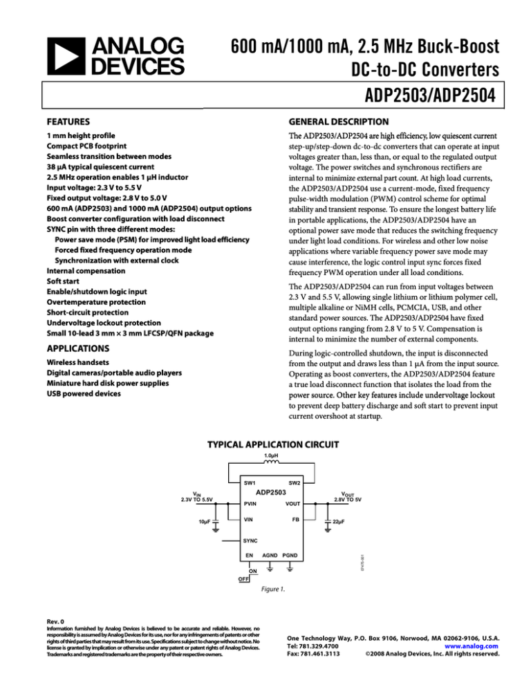
TYPICAL APPLICATION CIRCUIT
1.0µH
SW1
VIN
2.3V TO 5.5V
10µF
SW2
ADP2503
PVIN
VOUT
VIN
FB
VOUT
2.8V TO 5V
22µF
EN
AGND PGND
ON
07475-001
SYNC
OFF
Figure 1.
Rev. 0
Information furnished by Analog Devices is believed to be accurate and reliable. However, no
responsibility is assumed by Analog Devices for its use, nor for any infringements of patents or other
rights of third parties that may result from its use. Specifications subject to change without notice. No
license is granted by implication or otherwise under any patent or patent rights of Analog Devices.
Trademarks and registered trademarks are the property of their respective owners.
One Technology Way, P.O. Box 9106, Norwood, MA 02062-9106, U.S.A.
Tel: 781.329.4700
www.analog.com
Fax: 781.461.3113
©2008 Analog Devices, Inc. All rights reserved.
ADP2503/ADP2504
TABLE OF CONTENTS
Features .............................................................................................. 1
Soft Start ...................................................................................... 11
Applications ....................................................................................... 1
Sync Function ............................................................................. 11
General Description ......................................................................... 1
Enable........................................................................................... 11
Typical Application Circuit ............................................................. 1
Undervoltage Lockout ............................................................... 12
Revision History ............................................................................... 2
Thermal Shutdown .................................................................... 12
Specifications..................................................................................... 3
Short-Circuit Protection............................................................ 12
Absolute Maximum Ratings............................................................ 4
Reverse Current Limit ............................................................... 12
Thermal Resistance ...................................................................... 4
Applications Information .............................................................. 13
ESD Caution .................................................................................. 4
Inductor Selection ...................................................................... 13
Pin Configuration and Function Descriptions ............................. 5
PCB Layout Guidelines .................................................................. 15
Typical Performance Characteristics ............................................. 6
Outline Dimensions ....................................................................... 16
Theory of Operation ...................................................................... 11
Ordering Guide .......................................................................... 16
Power Save Mode........................................................................ 11
REVISION HISTORY
10/08—Revision 0: Initial Version
Rev. 0 | Page 2 of 16
ADP2503/ADP2504
SPECIFICATIONS
VIN = 3.6 V, VOUT = 3.3 V, @ TA = TJ = −40°C to +125°C for minimum/maximum specifications and TA = 25°C for typical specifications,
unless otherwise noted. 1
Table 1.
Parameters
INPUT CHARACTERISTICS
Input Voltage Range
Undervoltage Lockout Threshold
Undervoltage Lockout Threshold
OUTPUT CHARACTERISTICS
Output Voltage Range
Feedback Impedance
Output Voltage Initial Accuracy
Load and Line Regulation
CURRENT CHARACTERISTICS
Quiescent Current (VIN)
Shutdown Current
SWITCH CHARACTERISTICS
N-Channel Switches (LFCSP)
P-Channel Switches (LFCSP)
P-Channel Leakage
Switch Current Limit
ADP2504
ADP2503
Reverse Current Limit
OSCILLATOR AND STARTUP
Oscillator Frequency
On Time PMOS1 (Buck Mode)
On Time NMOS2 (Boost Mode)
Sync Clock Frequency
Sync Clock Minimum Off Time
LOGIC LEVEL CHARACTERISTICS
EN, SYNC Input High Threshold
EN, SYNC Input Low Threshold
EN, SYNC Leakage Current
THERMAL CHARACTERISTICS
Thermal Shutdown Threshold
Thermal Shutdown Hysteresis
1
Conditions
Min
Typ
Max
Unit
VIN rising
VIN falling
2.3
2.15
2.10
2.20
2.14
5.5
2.25
2.20
V
V
V
5.0
+2
0.5
0.6
V
kΩ
%
%
%
50
1
μA
μA
1
mΩ
mΩ
μA
2.0
1.4
1.1
A
A
A
2.9
MHz
ns
ns
MHz
ns
2.8
450
ADP2503/ADP2504 (PWM operation, no load)
VIN = 2.3 V to 3.6 V, ILOAD = 0 mA to 500 mA, forced PWM mode
VIN = 2.3 V to 5.5 V, ILOAD = 0 mA to 500 mA, forced PWM mode
−2
IOUT = 0 mA, V mode = EN = VIN = 3.6 V, device not switching
TA = TJ = −40°C to +85°C
38
0.2
VIN = 3.6 V
VIN = VOUT = 3.6 V
TJ = −40°C to +85°C
150
150
1.3
1.0
Minimum duty cycle = 30%
Maximum duty cycle = 50% (×2)
2.1
130
2.5
200
2.8
2.2
160
1.2
VIN = VEN
−1
+0.1
150
25
All limits at temperature extremes are guaranteed via correlation using standard statistical quality control (SQC).
Rev. 0 | Page 3 of 16
0.4
+1
V
V
μA
°C
°C
ADP2503/ADP2504
ABSOLUTE MAXIMUM RATINGS
THERMAL RESISTANCE
Table 2.
Parameter
PVIN, VIN, SW1, SW2, VOUT, SYNC,
EN, FB
PGND to AGND
Operating Ambient Temperature
Operating Junction Temperature
Storage Temperature
Lead Temperature
Soldering (10 sec)
Vapor Phase (60 sec)
Infrared (15 sec)
ESD Human Body Model
ESD Charged Device Model
ESD Machine Model
θJA is specified for a device soldered to a standard JEDEC2S2P
PCB. For a typical printed circuit board of a handset, the total
thermal resistance is higher. For correct operation up to 85°C
ambient temperature the total thermal resistance must not
exceed 100 K/W.
Rating
−0.3 V to +6 V
−0.3 V to 0.3 V
−40°C to +85°C
−40°C to +125°C
−65°C to +150°C
Table 3.
Package Type
10-Lead LFCSP (QFN)
300°C
215°C
220°C
±2000 V
±1500 V
±100 V
ESD CAUTION
Stresses above those listed under Absolute Maximum Ratings
may cause permanent damage to the device. This is a stress
rating only; functional operation of the device at these or any
other conditions above those indicated in the operational
section of this specification is not implied. Exposure to absolute
maximum rating conditions for extended periods may affect
device reliability.
Absolute maximum ratings apply individually only, not in
combination. Unless otherwise specified, all other voltages
are referenced to GND.
Rev. 0 | Page 4 of 16
θJA
84
Unit
°C/W
ADP2503/ADP2504
PIN CONFIGURATION AND FUNCTION DESCRIPTIONS
SW2 2
PGND 3
SW1 4
ADP2503/
ADP2504
TOP VIEW
(Not to scale)
PVIN 5
10 FB
9
AGND
8
VIN
7
SYNC
6
EN
*CONNECT PADDLE TO GND.
07475-003
VOUT 1
Figure 2. Pin Configuration
Table 4. Pin Function Descriptions
Pin No.
1
2
Mnemonic
VOUT
SW2
3
4
PGND
SW1
5
PVIN
6
7
EN
SYNC
8
9
10
EP
VIN
AGND
FB
Paddle
Description
Output of the ADP2503/ADP2504. Connect the output capacitor between VOUT and PGND.
Power Switch 2 Connection. This is the internal connection to the input PMOS and NMOS switches. Connect
SW2 to the inductor with a short, wide track.
Power GND. Connect the input and output capacitors and the PGND pin to a PGND plane.
Power Switch 1 Connection. This is the internal connection to the output PMOS and NMOS switches. Connect
SW1 to the inductor with a short, wide track.
Power Input. This the input to the buck-boost power switches. Place a 10 μF capacitor between PVIN and
PGND as close as possible to the ADP2503/ADP2504.
Enable. Drive EN high to turn on the ADP2503/ADP2504. Bring EN low to put the part into shutdown mode.
The SYNC pin permits the ADP2503/ADP2504 to operate in three different modes.
Normal operation: with SYNC driven low, the ADP2503/ADP2504 operate at 2.5 MHz PWM mode for heavy
and medium loads, and moves to power save mode (PSM) mode for light loads.
Forced PWM operation: with SYNC driven high, the ADP2503/ADP2504 operate at fixed 2.5 MHz PWM mode
for all load conditions.
SYNC mode: to synchronize the ADP2503/ADP2504 switching to an external signal, drive this pin with a clock
between 2.2 MHz and 2.8 MHz. The SYNC signal must have on and off times greater than 160 ns.
Analog Power Supply. This is the supply for the ADP2503/ADP2504 internal circuitry.
Analog Ground.
Output Feedback. This is an input to the internal error amplifier.
Connect the paddle to PGND.
Rev. 0 | Page 5 of 16
ADP2503/ADP2504
TYPICAL PERFORMANCE CHARACTERISTICS
700
100
90
600
70
EFFICIENCY (%)
VOUT = 2.8V
VOUT = 3.3V
VOUT = 3.5V
300
VOUT = 4.2V
VOUT = 4.5V
200
60
50
40
30
VOUT = 5.0V
VIN = 5.5V
VIN = 4.2V
VIN = 3.6V
VIN = 2.3V
20
100
10
2.3
2.8
3.3
3.8
4.3
INPUT VOLTAGE (V)
4.8
07475-114
0
5.3
Figure 3. ADP2503 Output Current vs. Input Voltage
0
0.001
1
Figure 6. Efficiency vs. Output Current, PSM and PWM Mode (VOUT = 5.0 V)
1100
100
90
900
80
800
70
EFFICIENCY (%)
700
VOUT = 2.8V
600
VOUT = 3.3V
500
VOUT = 3.5V
400
VOUT = 4.2V
VOUT = 4.5V
300
60
50
40
30
VOUT = 5.0V
200
20
100
10
2.3
2.8
3.3
3.8
4.3
INPUT VOLTAGE (V)
4.8
07475-115
0
5.3
0
0.001
0.01
0.1
1
IOUT (A)
Figure 4. ADP2504 Output Current vs. Input Voltage
Figure 7. Efficiency vs. Output Current, PWM Mode (VOUT = 3.3 V)
100
90
90
80
80
70
70
EFFICIENCY (%)
100
60
50
40
30
60
50
40
30
VIN = 5.5V
VIN = 4.2V
VIN = 3.6V
VIN = 2.3V
10
0.01
0.1
VIN = 5.5V
VIN = 4.2V
VIN = 3.6V
VIN = 2.3V
20
10
1
IOUT (A)
Figure 5. Efficiency vs. Output Current, PWM Mode (VOUT = 5.0 V)
07475-103
20
0
0.001
VIN = 5.5V
VIN = 4.2V
VIN = 3.6V
VIN = 2.3V
07475-109
OUTPUT CURRENT (A)
0.1
IOUT (A)
1000
EFFICIENCY (%)
0.01
07475-104
400
0
0.001
0.01
0.1
IOUT (A)
1
07475-108
OUTPUT CURRENT (A )
80
500
Figure 8. Efficiency vs. Output Current, PSM and PWM Mode (VOUT = 3.3 V)
Rev. 0 | Page 6 of 16
ADP2503/ADP2504
100
3.35
90
80
3.33
60
VOUTA (V)
EFFICIENCY (%)
70
50
40
3.31
3.29
30
VIN = 5.5V
VIN = 4.2V
VIN = 3.6V
VIN = 2.3V
0
0.001
0.01
0.1
1
IOUT (A)
07475-110
10
3.27
07475-105
20
3.25
0
0.1
0.2
0.3
0.4
0.5
0.6
0.7
0.8
0.9
1.0
IOUT (A)
Figure 9. Efficiency vs. Output Current, PWM Mode (VOUT = 2.8 V)
Figure 12. Load Regulation (VIN = 3.6 V, VOUT = 3.3 V)
100
2.8
90
2.7
80
–40°C
FREQUENCY (MHz)
60
50
40
30
VIN = 5.5V
VIN = 4.2V
VIN = 3.6V
VIN = 2.3V
0
0.001
0.01
2.4
0.1
1
2.2
2.3
Figure 10. Efficiency vs. Output Current, PSM and PWM Mode (VOUT = 2.8 V)
45
80
40
QUIESCENT CURRENT (µA)
50
90
70
60
50
40
30
IOUT = 500mA
IOUT = 100mA
IOUT = 10mA
3.1
3.5
3.9
VIN (V)
4.3
4.7
5.1
5.5
35
30
25
20
15
10
10
5
2.8
3.3
3.8
VIN (V)
4.3
4.8
5.3
07475-107
0
2.3
2.7
Figure 13. Frequency vs. Input Voltage Over Temperature (VOUT = 3.3 V)
100
20
+85°C
2.3
IOUT (A)
EFFICIENCY (%)
+25°C
2.5
07475-112
10
07475-106
20
2.6
0
2.3
Figure 11. Efficiency vs. Input Voltage (VOUT = 3.3 V)
2.7
3.1
3.5
3.9
VIN (V)
4.3
4.7
5.1
5.5
Figure 14. Quiescent Current vs. Input Voltage (VOUT = 3.3 V)
Rev. 0 | Page 7 of 16
07475-113
EFFICIENCY (%)
70
ADP2503/ADP2504
VIN
VIN = 3.0V TO 3.6V
VOUT = 5.0V
VIN = 3.6V
VOUT = 3.3V
VOUT
1
SW1
IOUT
2
4
SW2
2
SW1
3
4
VOUT
07475-005
CH1 50.0mV BW CH2 1.00V BW M40.0µs A CH2
CH3 5.00V BW
CH4 5.00V BW T 18.20%
3
3.40mV
CH1 100mV BW CH2 250mA Ω M100µs
A CH2
CH3 5.00V BW CH4 5.00V BW T 25.80%
Figure 15. Line Transient, PWM Mode (VIN = 3.0 V to 3.6 V, VOUT = 5.0 V)
VIN
07475-008
SW2
1
60.0mA
Figure 18. Load Transient (VIN = 3.6 V VOUT = 3.3 V, IOUT = 100 mA to 350 mA)
VIN = 3.0V TO 3.6V
VOUT = 3.3V
VIN = 3.6V
VOUT = 3.3V
1
VOUT
IOUT
SW1
2
4
SW2
2
SW1
3
4
VOUT
07475-006
CH1 50.0mV
CH3 5.00V BW
B
B
A CH2
W CH2 1.00V W M40.0µs
CH4 5.00V BW T 18.20%
3
CH1 100mV BW CH2 250mA Ω M100µs
A CH2
CH3 5.00V BW
CH4 5.00V BW T 23.00%
3.40V
Figure 16. Line Transient, PWM Mode (VIN = 3.0 V to 3.6 V, VOUT = 3.3 V)
VIN
07475-111
SW2
1
60.0mA
Figure 19. Load Transient (VIN = 3.6 V VOUT = 3.3 V, IOUT = 10 mA to 300 mA)
VIN = 3.0V TO 3.6V
VOUT = 2.8V
SW1
SW1
4
4
2
IOUT
SW2
2
3
VOUT
07475-007
1
CH1 50.0mV BW CH4 1.00V BW M40.0µs
A CH2
CH3 5.00V BW
CH4 5.00V BW T 18.20%
VIN = 3.6V
VOUT = 3.3V
07475-010
VOUT
1
3.40mV
CH1 100mV BW CH2 500mA Ω
CH4 2.00V BW
Figure 17. Line Transient, PWM Mode (VIN = 3.0 V to 3.6 V, VOUT = 2.8 V)
Rev. 0 | Page 8 of 16
M100µs
A CH2
T 45.40%
–115mA
Figure 20. Mode Change by Load Transients, Load Rise (VOUT = 3.3 V)
ADP2503/ADP2504
SW1
SW2
VIN = 3.0V
VOUT = 3.3V
3
SW1
4
4
IOUT
ISW
2
VIN = 3.6V
VOUT = 3.3V
VOUT
CH1 100mV BW CH2 500mA Ω
CH4 2.00V BW
1
M100µs
A CH2
T 45.40%
CH1 20.0mV BW CH2 250mA Ω
410mA
CH3 5.00V BW
CH4 5.00V BW
M 400ns
A CH4
T 50.00%
2.40V
Figure 24. Typical PWM Switching Waveform, Buck-Boost Operation
(VOUT = 3.3 V)
Figure 21. Mode Change by Load Transients, Load Fall (VOUT = 3.3 V)
SW2
07475-027
VOUT
1
07475-011
2
VIN = 3.0V
VOUT = 3.3V
VIN = 4.0V
VOUT = 3.3V
SW2
3
3
SW1
SW1
4
4
ISW
ISW
2
2
VOUT
VOUT
07475-012
CH1 50.0mV BW CH2 250mA Ω
CH3 5.00V BW
CH4 5.00V BW
M 400ns
A CH3
T 50.00%
CH1 100mV BW CH2 1.00A Ω
2.40V
CH3 5.00V BW
Figure 22. Typical PWM Switching Waveform, Buck Operation (VOUT = 3.3 V)
SW2
07475-015
1
1
CH4 5.00V BW
M 4.00µs
A CH2
T 15.20%
820mA
Figure 25. Typical PSM Switching Waveform, Buck-Boost Operation
(VOUT = 3.3 V)
VIN = 3.0V
VOUT = 3.3V
SW1
4
3
SW1
VOUT = 3.3V
VOUT
4
1
ISW
ISW
2
2
EN
VOUT
CH1 20.0mV BW CH2 250mA Ω
CH3 5.00V BW
CH4 5.00V BW
M 400ns
A CH4
T 50.80%
07475-018
3
07475-013
1
CH1 2.00V BW CH2 500mAΩ BW M 100µs
A CH3
T 9.400%
CH3 5.00V BW CH4 5.00V BW
2.40V
Figure 23. Typical PWM Switching Waveform, Boost Operation (VOUT = 3.3 V)
Rev. 0 | Page 9 of 16
2.40V
Figure 26. Startup into PWM Mode (VOUT = 3.3 V, IOUT = 300 mA)
ADP2503/ADP2504
SW1
SW1
4
4
VOUT
VOUT
VOUT = 3.3V
1
VOUT = 3.3V
1
ISW
ISW
2
2
EN
EN
CH1 2.00V BW CH2 500mAΩ BW M 100µs
A CH3
T 9.400%
CH3 5.00V BW CH4 5.00V BW
07475-023
3
07475-019
3
CH1 2.00V BW CH2 500mAΩ BW M 100µs
A CH3
T 9.400%
CH3 5.00V BW CH4 5.00V BW
2.40V
Figure 27. Startup into PWM Mode (VOUT = 3.3 V, IOUT = 10 mA)
2.40V
Figure 28. Startup into PSM Mode (VOUT = 3.3 V, IOUT = 10 mA)
Rev. 0 | Page 10 of 16
ADP2503/ADP2504
THEORY OF OPERATION
1.0µH
SW1
SW2
4
ADP2503/ADP2504
VIN
ADP2503/ADP2504
BIASING
8
VBAT = 2.3V
TO 5.5V
2
PMOS1
PVIN
PMOS2
VOUT
5
1
10µF
NMOS1
22µF
NMOS2
2.25V
SOFT START
UVLO
FB
BAND GAP
REFERENCE
10
THERMAL
PROTECTION
–0.5V
PWM CONTROL
EN
EN
6
SYNC
OSCILLATOR
PGND
AGND
3
9
07475-025
7
CS
Figure 29. ADP2503/ADP2504 Block Diagram
The ADP2503/ADP2504 are synchronous average currentmode switching buck-boost regulators designed to maintain a
fixed output voltage VOUT from an input supply VIN that can be
greater than, equal to, or less than VOUT. When VIN is significantly greater than VOUT, the device is in buck mode: PMOS2 is
always active, NMOS2 is always off, and the PMOS1, NMOS1
switches constitute a buck converter. When VIN is significantly
lower than VOUT, the device is in boost mode: PMOS1 is always
active, NMOS1 is always off, and the NMOS2, PMOS2 switches
constitute a boost converter. When VIN is in the range [VOUT −
10%; VOUT + 10%], the ADP2503/ADP2504 automatically enter
the buck-boost mode. In buck-boost mode, the two operations
buck (PMOS1 and NMOS1 switching in antiphase) and boost
(NMOS2 and PMOS2 switching in antiphase) take place at each
period of the clock. This is aimed at maintaining the regulation
and keeping a minimal current ripple in the inductor to
guarantee good transient performances.
POWER SAVE MODE
When the SYNC pin is low, the ADP2503/ADP2504 can operate
in power save mode (PSM). In this mode, when the load current
becomes less than 75 mA nominally at VIN = 3.6 V, the controller pulls up VOUT and then halts the switching regime until
VOUT goes back to a restart value. Then VOUT is pulled up again
for a new cycle. This minimizes the switching losses at light load.
When the load rises above 150 mA, the ADP2503/ADP2504 revert
to fixed PWM mode. This results in about 75 mA of hysteresis
between PSM and fixed PWM, preventing oscillations between
these two modes.
SOFT START
When the ADP2503/ADP2504 are started, VOUT is ramped from
0 V to its final programmed value in 200 μs (typ). This limits
the inrush current to less than 600 mA for a nominal output
capacitor of 20 μF. Because the VOUT start-up slope is constant,
the inrush current becomes larger if the output capacitor is
made larger.
SYNC FUNCTION
When the SYNC pin is high, PSM is deactivated. The ADP2503/
ADP2504 always operate in PWM using the internal oscillator.
When the SYNC pin is switching in the 2.2 MHz to 2.8 MHz
range, the regulator switching frequency slides to the fre-
quency applied on SYNC and then locks on it. When the
SYNC pin stops switching, the regulator switching frequency
slides back to the internal oscillator frequency.
ENABLE
The device starts operation with soft start when the EN pin
is brought high. Pulling the EN pin low forces the device into
shutdown, with a typical shutdown current of 0.2 μA.
In this mode, the PMOS power switches are turned off, the
NMOS power switches are turned on, and the control circuitry
is not enabled. For proper operation, the EN pin must be
terminated and must not be left floating.
Rev. 0 | Page 11 of 16
ADP2503/ADP2504
UNDERVOLTAGE LOCKOUT
SHORT-CIRCUIT PROTECTION
The undervoltage lockout circuit prevents the device from operating incorrectly at low input voltages. It prevents the converter
from turning on the power switches under undefined conditions
and, therefore, prevents deep discharge of the battery supply.
VIN must be greater than 2.25 V to enable the converter. During
operation, if VIN drops below 2.18 V, the ADP2503/ADP2504
are disabled until the supply exceeds the UVLO rising threshold.
When the nominal inductor peak current value of 1.5 A is
reached, the ADP2503/ADP2504 first switch off the NMOS2
transistor if it was active. If the current thereafter continues to
increase by an extra amount of 200 mA, the PMOS1 transistor
is also switched off. This operation is reversible when the short
circuit stops. It allows the inductor current ripple to be minimized close to 1.5 A and, thus, the controller to restore VOUT
even if a high load current is maintained after the short circuit.
THERMAL SHUTDOWN
When the junction temperature, TJ, exceeds 150°C typical,
the device goes into thermal shutdown. In this mode, the power
switches are turned off. The device resumes operation when the
junction temperature again falls below 125°C typical.
REVERSE CURRENT LIMIT
In case of a short circuit on VOUT to a value greater than
expected, the inductor current becomes negative (reverse
current). The negative peak value is limited to 1.1 A by
deactivating the switch PMOS2.
Rev. 0 | Page 12 of 16
ADP2503/ADP2504
APPLICATIONS INFORMATION
INDUCTOR SELECTION
Table 5. Sample of Recommended Inductors
The high 2.5 MHz switching frequency of the ADP2503/
ADP2504 allows for minimal output voltage ripple, while
minimizing inductor size and cost. Careful inductor selection
also optimizes efficiency and reduces electromagnetic interference (EMI). The selection of the inductor value determines
the inductor current ripple and loop dynamics.
ΔI L , peak (Buck) =
VOUT × (VIN − VOUT )
ΔI L , peak ( Boost ) =
VIN × f OSC × L
(VOUT − V IN )
VOUT
×
VIN
f OSC × L
where fOSC is the switching frequency (typically 2.5 MHz),
and L is the inductor value in henries.
A larger inductor value reduces the current ripple (and, therefore,
peak inductor current), but is physically larger in size with
increased dc resistance. Inductor values between 1 μH and
1.5 μH are usually suggested. The maximum inductor value
to ensure stability is 2.0 μH. For increased efficiency with the
ADP2504, it is suggested that a 1.5 μH inductor be used.
Vendor
Toko
Toko
Toko
Murata
Murata
TDK
TDK
Coilcraft
Coilcraft
Taiyo
Yuden
⎞ 1
⎟×
⎟ η
⎠
Part No.
DE2810C
DE2810C
MDT2520-CN
LQM2HP-G0
LQM2HP-G0
CPL2512T
CPL2512T
LPS3010
LPS3010
NR3015T1
DCR
(mΩ)
55
60
100
55
70
90
120
85
120
40
The saturation current rating of the inductor must be at least
IIN(MAX) + ΔILOAD/2.
Ceramic multilayer inductors can be used with lower current
designs for a reduced overall solution size and dc resistance
(DCR). These are available in low profile packages. Care must
be taken because these derate quickly as the inductor value is
increased, especially at higher operating temperatures.
The output capacitor selection determines the output voltage
ripple, transient response, and the loop dynamics of the
ADP2503/ADP2504. The output voltage ripple for a given
output capacitor is given by
ΔVOUT , peak ( Buck) =
ΔVOUT , peak (Boost ) =
VOUT × (V IN − VOUT )
V IN × 8 × L × ( f OSC )2 × C OUT
I LOAD × (VOUT − V IN )
C OUT × VOUT × f OSC
The maximum voltage overshoot, or undershoot, is inversely
proportional to the value of the output capacitor. To ensure
stability and excellent transient response, it is recommended
to use a minimum of 22 μF X5R 6.3 V or 2 × 10 μF X5R 6.3 V
capacitors at the output. The effective capacitance (includes
temperature and dc bias effects) needed for stability is 14 μF.
Ferrite core inductors have good core loss characteristics as well as
reasonable dc resistance. A shielded ferrite inductor reduces the
EMI generated by the inductor.
Table 6. Recommended Output Capacitors
Value
2 × 10 μF, 6.3 V
2 × 10 μF, 6.3 V
22 μF, 6.3 V
22 μF, 6.3 V
22 μF, 10 V
10 μF, 10 V
Dimensions
L ×W × H
(mm)
2.8 × 2.8 × 1.0
2.8 × 2.8 × 1.0
2.5 × 2 × 1.2
2.5 × 2 × 1
2.5 × 2 × 1
2.5 × 1.5 × 1.2
2.5 × 1.5 × 1.2
3.0 × 3.0 × 0.9
3.0 × 3.0 × 0.9
3.0 × 3.0 × 1.5
If the ADP2503/ADP2504 are operating in buck mode, the
worst-case voltage ripple occurs for the highest input voltage,
VIN. If the ADP2503/ADP2504 are operating in boost mode, the
worst-case voltage ripple occurs for the lowest input voltage, VIN.
where η is efficiency (assume η ≈ 0.85 to 0.90).
Vendor
Murata
TDK
Murata
TDK
TDK
Murata
ISAT
(A)
1.7
1.5
1.8
1.6
1.5
1.5
1.2
1.7
1.3
1.5
Output Capacitor Selection
The inductor peak current is at the maximum in boost mode.
To determine the actual maximum inductor current in boost
mode, the input dc current should be estimated.
⎛V
I IN ( MAX ) = I LOAD( MAX ) × ⎜⎜ OUT
⎝ VIN
Value
(μH)
1.2
1.5
1
1
1.5
1.0
1.5
1.0
1.5
1.5
Part No.
GRM188R60J106ME47
C1608JB0J106K
GRM21BR60J226ME39
C2012X5R0J226M
C3216X5R1A226K
GRM21BR71A106KE51L
Rev. 0 | Page 13 of 16
Dimensions
L × W × H (mm)
1.6 × 0.8 × 0.8 (2)
1.6 × 0.8 × 0.8 (2)
2 × 1.25 × 1.25
2 × 1.25 × 1.25
2 × 1.25 × 1.25
2 × 1.25 × 1.25 (2)
ADP2503/ADP2504
Input Capacitor Selection
Table 7. Recommended Input Capacitors
The ADP2503/ADP2504 require an input capacitor to filter
noise on the VIN pin, and provide the transient currents while
maintaining constant input and output voltage. A 10 μF X5R/
X7R ceramic capacitor rated for 6.3 V is the minimum recommended input capacitor. Increased input capacitance reduces
the amplitude of the switching frequency ripple on the battery.
Because of the dc bias characteristics of ceramic capacitors, a
0603, 6.3 V X5R/X7R, 10 μF ceramic capacitor is preferable.
Vendor
Murata
TDK
Rev. 0 | Page 14 of 16
Value
10 μF, 6.3 V
10 μF, 6.3 V
Part No.
GRM188R60J106ME47
C1608JB0J106K
Dimensions
L×W×H
(mm)
1.6 × 0.8 × 0.8
1.6 × 0.8 × 0.8
ADP2503/ADP2504
PCB LAYOUT GUIDELINES
Poor layout can affect ADP2503/ADP2504 performance, causing electromagnetic interference (EMI) and electromagnetic
compatibility (EMC) performance, ground bounce, and voltage
losses. Poor layout can also affect regulation and stability. A good
layout is implemented using the following rules:
•
•
Place the inductor, input capacitor, and output capacitor
close to the IC using short tracks. These components carry
high switching frequencies and large tracks act like antennas.
Route the output voltage path away from the inductor and
SW node to minimize noise and magnetic interference.
Maximize the size of ground metal on the component side
to help with thermal dissipation.
Use a ground plane with several vias connecting to the
component side ground to further reduce noise interference
on sensitive circuit nodes.
07475-026
•
•
Figure 30. ADP2503/ADP2504 Evaluation Board
Rev. 0 | Page 15 of 16
ADP2503/ADP2504
OUTLINE DIMENSIONS
0.30
0.23
0.18
0.50 BSC
10
6
PIN 1 INDEX
AREA
1.74
1.64
1.49
*EXPOSED
PAD
(BOTTOM VIEW)
0.50
0.40
0.30
5
TOP VIEW
2.48
2.38
2.23
0.80 MAX
0.55 NOM
0.80
0.75
0.70
1
0.05 MAX
0.02 NOM
SEATING
PLANE
PIN 1
INDICATOR
(R 0.20)
*PADDLE CONNECTED TO GND.
0.20 REF
060408-B
3.00
BSC SQ
Figure 31. 10-Lead Lead Frame Chip Scale Package [LFCSP_WD]
3 mm × 3 mm Body, Very Very Thin, Dual Lead
(CP-10-9)
Dimensions shown in millimeters
ORDERING GUIDE
Model
ADP2503ACPZ-2.8-R7 1
ADP2503ACPZ-3.3-R71
ADP2503ACPZ-3.5-R71
ADP2503ACPZ-4.2-R71
ADP2503ACPZ-4.5-R71
ADP2503ACPZ-5.0-R71
ADP2504ACPZ-2.8-R71
ADP2504ACPZ-3.3-R71
ADP2504ACPZ-3.5-R71
ADP2504ACPZ-4.2-R71
ADP2504ACPZ-4.5-R71
ADP2504ACPZ-5.0-R71
ADP2503-2.8-EVAL-Z1
ADP2503-3.3-EVAL-Z1
ADP2503-3.5-EVAL-Z1
ADP2503-4.2-EVAL-Z1
ADP2503-4.5-EVAL-Z1
ADP2503-5.0-EVAL-Z1
ADP2504-2.8-EVAL-Z1
ADP2504-3.3-EVAL-Z1
ADP2504-3.5-EVAL-Z1
ADP2504-4.2-EVAL-Z1
ADP2504-4.5-EVAL-Z1
ADP2504-5.0-EVAL-Z1
1
Voltage
2.8 V
3.3 V
3.5 V
4.2 V
4.5 V
5.0 V
2.8 V
3.3 V
3.5 V
4.2 V
4.5 V
5.0 V
Maximum
Current
0.6 A
0.6 A
0.6 A
0.6 A
0.6 A
0.6 A
1A
1A
1A
1A
1A
1A
Temperature
Range
−40°C to +85°C
−40°C to +85°C
−40°C to +85°C
−40°C to +85°C
−40°C to +85°C
−40°C to +85°C
−40°C to +85°C
−40°C to +85°C
−40°C to +85°C
−40°C to +85°C
−40°C to +85°C
−40°C to +85°C
Package Description
10-Lead Lead Frame Chip Scale Package [LFCSP_WD]
10-Lead Lead Frame Chip Scale Package [LFCSP_WD]
10-Lead Lead Frame Chip Scale Package [LFCSP_WD]
10-Lead Lead Frame Chip Scale Package [LFCSP_WD]
10-Lead Lead Frame Chip Scale Package [LFCSP_WD]
10-Lead Lead Frame Chip Scale Package [LFCSP_WD]
10-Lead Lead Frame Chip Scale Package [LFCSP_WD]
10-Lead Lead Frame Chip Scale Package [LFCSP_WD]
10-Lead Lead Frame Chip Scale Package [LFCSP_WD]
10-Lead Lead Frame Chip Scale Package [LFCSP_WD]
10-Lead Lead Frame Chip Scale Package [LFCSP_WD]
10-Lead Lead Frame Chip Scale Package [LFCSP_WD]
Evaluation Board for 2.8 V
Evaluation Board for 3.3 V
Evaluation Board for 3.5 V
Evaluation Board for 4.2 V
Evaluation Board for 4.5 V
Evaluation Board for 5.0 V
Evaluation Board for 2.8 V
Evaluation Board for 3.3 V
Evaluation Board for 3.5 V
Evaluation Board for 4.2 V
Evaluation Board for 4.5 V
Evaluation Board for 5.0 V
Z = RoHS Compliant Part.
©2008 Analog Devices, Inc. All rights reserved. Trademarks and
registered trademarks are the property of their respective owners.
D07475-0-10/08(0)
Rev. 0 | Page 16 of 16
Package
Option
CP-10-9
CP-10-9
CP-10-9
CP-10-9
CP-10-9
CP-10-9
CP-10-9
CP-10-9
CP-10-9
CP-10-9
CP-10-9
CP-10-9
Branding
L9Y
L9Z
LAP
LA0
LA1
LA2
L9T
L85
LAN
L9U
L9V
L9W
