Progress on Silicon-on-Insulator Monolithic Pixel Process
advertisement
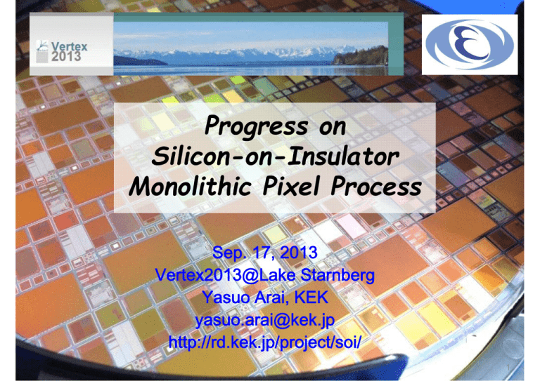
Progress on Silicon-on-Insulator Monolithic Pixel Process Sep. 17, 2013 Vertex2013@Lake Starnberg Yasuo Arai, KEK yasuo.arai@kek.jp http://rd.kek.jp/project/soi/ 1 Outline • • • • • Introduction Basic SOI Pixel Process Advanced Process Techniques Project Status Summary 2 Introduction Silicon-On-Insulator Pixel Detector (SOIPIX) 3 Feature of SOI Pixel Detector • No mechanical bonding. Fabricated with semiconductor process only, so high reliability, low cost are expected. • Fully depleted thick sensing region with Low sense node capacitance. • On Pixel processing with CMOS transistors. • Can be operated in wide temperature (1K-570K) range, and has low single event cross section. • Based on Industry Standard Technology. 4 Regular Multi-Project Wafer (MPW) run. (~twice/year) JAXA Fermi Nat'l Accl. Lab. RIKEN Osaka U. Tohoku U. KEK Lawrence Berkeley Nat'l Lab. AGH & IFJ, Krakow U. Heidelberg Louvain Univ. AIST Kyoto U. Tsukuba U. IHEP/IMECAS/SARI China SOIPIX MPW run Wafer 5 Basic SOI Pixel Process 6 Lapis (*) Semi 0.2 m FD-SOI Pixel Process Process 0.2m Low-Leakage Fully-Depleted SOI CMOS 1 Poly, 5 Metal layers. MIM Capacitor (1.5 fF/um2), DMOS Core (I/O) Voltage = 1.8 (3.3) V SOI wafer Diameter: 200 mm, 720 m thick Top Si : Cz, ~18 -cm, p-type, ~40 nm thick Buried Oxide: 200 nm thick Handle wafer: Cz (n) ~700 -cm, FZ(n) ~7k -cm, FZ(p) ~25 k -cm etc. Backside Mechanical Grind, Chemical Etching, Back side process Implant, Laser Annealing and Al plating (*) Former OKI Semiconductor Co. Ltd. 7 Mask Size 24.6 x 30.8 mm Smallest chip area for MPW run is 2.9mm x 2.9mm 8 Structure of Top Si 1 Poly + 5 Metal MIM Capacitor on 3M 9 Structure of Bottom Si (Sensor part) • PS & NS --- High doping density Layer (Top Si is removed) • Buried Well (BPW, BP2, BP3 & BNW ) --- Low doping density buried Layer • For p-type substrate, dopants are changed to create reverse polarity by using the same mask layers. • Doping density and depth can be changed on request. 10 An example of SOIPIX: Integration Type Pixel (INTPIX) Pixel Size : 12x12 m2 896x1408 (~1.3 M)pixels、 11 Analog out port、Column CDS. 12.2 mm 18.4 mm INTPIX5 11 Examples of SOIPIX Measurement PF-AR NE7A 33.3keV monochromatic Acrylic resin 40mm 200us x 250 frames RA Arb. unit 8700 Needle 8.704mm Acrylic Resin Stent Wire (INTPIX4) -46000 14.144mm CA 12 Examples of SOIPIX Measurement Compton Electron Tracks X-ray Energy Spectrum@-50℃ noise 18e- rms 13 Advanced Process Techniques • Stitching • Double SOI • 3D Vertical Integration 14 Stitching Exposure for Large Sensor SOPHIAS by RIKEN Reticule size ~25mm x 31mm Buffer Region 10um Shot A Shot A Buffer Region 10um Shot A Shot B • Width of the Buffer Region can be less than 10um. • Accuracy of Overwrap is better than 0.025um. 15 16 Double SOI wafer Sensor and Electronics are located very near. This cause .. BPW At first, we successfully introduced BPW layer to remove the back gate effect. Then we newly introduced additional conductive layer under the transistors to reduce all effects ( Double SOI). 17 Double SOI Process Middle Si Layer (SOI2) SOI2 PS2 18 First Trial : Double-SOI from SOITEC Si:46.7nm SiO2:158.7nm Si:84nm SiO2:156.0nm Poly-Si Top-Si BOX1(SiO2) Middle-Si BOX2(SiO2) Handle-Wafer (after Field-Anneal) Resistivity of the middle Si is ~10 Ohm•cm. with CoSi2 : ~170 kOhm/ w/o CoSi2 : ~1 MOhm/ 19 Negative View Transistor Gate Top-SOI Sensor Contact BOX2 BOX1 Sub Middle-SOI 0.3um 20 Suppression of Back-Gate Effect with Middle-Si layer b) Middle-Si = GND 1.0E-03 1.0E-03 1.0E-04 1.0E-04 1.0E-05 1.0E-05 1.0E-06 1.0E-06 1.0E-07 1.0E-07 Vback=0V Vback=5V Vback=10V Vback=15V Vback=20V Vback=25V 1.0E-08 1.0E-09 1.0E-10 1.0E-11 1.0E-12 -0.5 Ids [A] Ids [A] a) Middls-Si Floating 0 0.5 1 Vg [V] 1.5 Vback=0V Vback=100V Vback=200V Vback=300V Vback=400V Vback=500V 1.0E-08 1.0E-09 1.0E-10 1.0E-11 2 1.0E-12 -0.5 Back-Gate Effect is fully suppressed with the Middle Si Layer of fixed voltage. 0 0.5 1 Vg [V] 1.5 2 Nch Core Normal-Vt L / W = 0.2 / 5.0um Vd=0.1V 21 Gamma-ray Irradiation Test (Id-Vg Characteristics v.s. SOI2 Potential) I/O normal Vth Source-Tie Tr. L/W =0.35um/5um NMOS 10Mrad 0 kGy Vg[V] VSOI2=-5V Id[A] VSOI2=-2V Id[A] Id[A] VSOI2=0V 10Mrad 0 kGy 0 kGy Vg[V] Vg[V] By setting Vsoi2 ~ -5V, Id-Vg curve returned nearly to pre-irradiation value. 22 Variation of Id-Vg Characteristics and Effect of SOI2 Potential I/O Normal Vt Source-Tie L/W =0.35um/5um PMOS 0 kGy VSOI2=-5V Id[A] VSOI2=-2V Id[A] Id[A] VSOI2=0V 0 kGy 0 kGy 10Mrad 10Mrad Vg[V] Vg[V] Vg[V] The VSOI2 effect to PMOS is not so large compared to NMOS case. Id-Vg curve also returned to pre-irradiation value @VSOI2~-5V. 23 Necessary VSOI2 voltage to restore original threshold voltage Preliminary! ? 10 Mrad 24 Effect of Middle Si potential to Charge Collection VSENSE=1V VSOI2=0V n- VBACK=50V VSOI2=-2V • To compensate trapped hole effect, negative SOI2 voltage is necessary. • To push electrical flux lines to sense node positive SOI2 voltage is necessary. It is better to use p-type substrate instead of ntype. 25 New DSOI Wafer SOITEC Shinetsu (next run) • Substrate is changed from n-type to p-type to have better field shape. • Thickness of SOI2 is doubled to have lower resistance. • Type of SOI2 layer is changed to n-type not to deplete the layer. • Supplier is also changed. 26 Vertical (3D) Integration 3D vertical Integration technique is expected to play an important role in future high performance pixel detector. We have made 3D test chips. These chips were bonded with -bump technology (~5 um pitch) of T-micro Co. Ltd. 27 28 Daisy Chain TEG (After Deposition) Alignment Mark (After Stacking – Adhesive Injection – Si Wet Etching) Upper Chip Lower Chip 29 Preliminary! Id – Vd Characteristcs NMOS Source-Tie w/l=32u/0.35u PMOS Body-Tie w/l=50u/0.35u Upper Upper Lower Lower Id-Vd characteristic looks different between upper and lower tiers. 30 Project Status Diffraction Enhanced (Low angle) Image (a kidney bean) 31 On-Going SOI Projects in Japan • INTPIX : Genera Purpose Integration Type KEK • SOPHIAS : Large Dynamic Range for XFEL Riken • PIXOR : Belle II Vertex Detector Tohoku Univ. • XRPIX : X-ray Astronomy in Satellite Kyoto Univ. • STJPIX : Superconducting Tunnel Junction on SOI Tsukuba Univ. • CNTPIX : General Purpose Counting Type KEK • LHDPIX : Nuclear Fusion Plasma X-ray KEK, NIFS • MALPIX : TOF Imaging Mass Spectrometer KEK, Osaka Univ. • TDIPIX : Time Delaying Integration for X-ray Inspection KEK •… and Many Other Project are being planned 32 SOI project of 5 years is granted! 【Term of Project】 FY2013-2017 【Budget Allocation】 ~$10M 33 Summary • We have been developing SOI Pixel process and fabricated many kinds of SOIPIX detectors which integrate both radiation sensors and readout circuits in a single die. • We have ~twice/year regular MPW runs with increasing No. of users. • Many new process technologies have been developed; Buried P-well, High resistive SOI wafer, Nested well structure, Stitching, Double SOI, Vertical integration … • Double SOI of p-type substrate looks promising for radhard counting-type pixel detector. • New SOI project of 5 year period is approved by Japanese government. 34
