MGPA – Power Supply Rejection Mark Raymond (1/2/03

MGPA – Power Supply Rejection Mark Raymond (1/2/03)
Introduction
The highest priority area to be investigated following the design review of January
13 th
was the power supply rejection (PSR) where no rejection (actually gain) was demonstrated at frequencies around 100 Hz. Since then I have been investigating the origins of the problem, seeking improvements which don’t require changes to the core architecture where simulations show adequate performance in other respects. It is of course likely that PSR could be improved by changes to the core architecture, but these would only come at the cost of increased noise, complexity (risk), power, and also a significant delay to the chip submission.
There is no specification for PSR, which should be defined by the environment in which the chip will operate. My understanding is that this environment (e.g. temperature) will be rather stable, for reasons associated with the crystal/APD performance, and that power supplies will be locally regulated. I expect therefore that power supply DC stability will be rather good. Pick-up from local digital activity can be minimised by careful layout and local RC filtering of supply voltages to the MGPA with time constants ~ 10 – 100
µ s. Power supply noise will also be subject to this local filtering. I note that the rad-hard voltage regulators developed by the RD49 collaboration have a measured noise performance of ~300
µ
V rms in a 10 Hz – 10
MHz bandwidth. The MGPA differential output of 1.8 Volts leads to an LSB value
(12 bits) of 400
µ
V. The magnitudes of these figures can help when judging the requirements of the MGPA PSR performance.
Design factors affecting PSR and improvements achieved
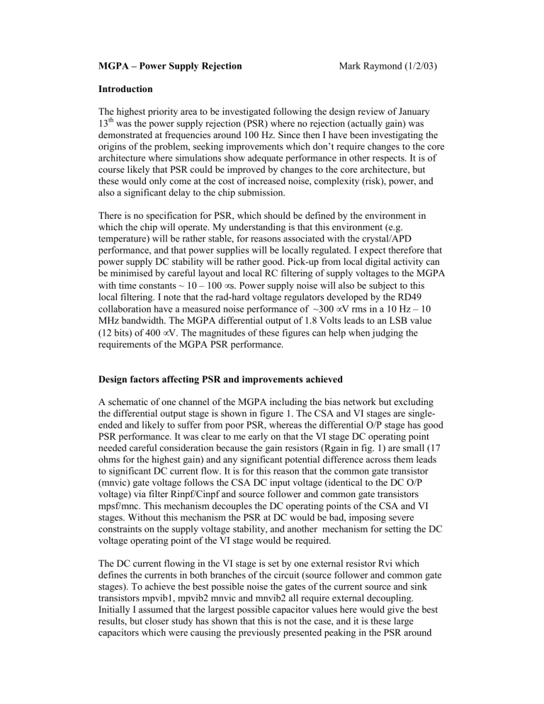
A schematic of one channel of the MGPA including the bias network but excluding the differential output stage is shown in figure 1. The CSA and VI stages are singleended and likely to suffer from poor PSR, whereas the differential O/P stage has good
PSR performance. It was clear to me early on that the VI stage DC operating point needed careful consideration because the gain resistors (Rgain in fig. 1) are small (17 ohms for the highest gain) and any significant potential difference across them leads to significant DC current flow. It is for this reason that the common gate transistor
(mnvic) gate voltage follows the CSA DC input voltage (identical to the DC O/P voltage) via filter Rinpf/Cinpf and source follower and common gate transistors mpsf/mnc. This mechanism decouples the DC operating points of the CSA and VI stages. Without this mechanism the PSR at DC would be bad, imposing severe constraints on the supply voltage stability, and another mechanism for setting the DC voltage operating point of the VI stage would be required.
The DC current flowing in the VI stage is set by one external resistor Rvi which defines the currents in both branches of the circuit (source follower and common gate stages). To achieve the best possible noise the gates of the current source and sink transistors mpvib1, mpvib2 mnvic and mnvib2 all require external decoupling.
Initially I assumed that the largest possible capacitor values here would give the best results, but closer study has shown that this is not the case, and it is these large capacitors which were causing the previously presented peaking in the PSR around
100 Hz. Transient simulations show that if the supply voltage changes the bias circuit adjusts its operating point appropriately, but during the settling time relatively large transients occur at the VI stage current output where one LSB is equivalent to 0.55
µ
A. Large decoupling capacitor values prolong the settling time duration and so these should be reduced. The settling time can also be reduced by reducing impedances in the bias circuit so I have doubled the widths and currents in the bias transistors which also helps to reduce their noise. This results in an increase in power consumption of ~
40 mW. The decoupling capacitors Cd1, Cd2 and Cd3 are now 2.2
µ
F, 22n and 22n respectively. Settling time can be further reduced by the addition of capacitors Cd4,
Cd5 and Cd6. Cd4 reduces the settling time at the gate (and drain) node of mpb1 as the Cd4.[1/gm(mpb1)] time constant compensates for the Cd1.Rvi time constant. Cd5 and Cd6 speed up the settling at the gates of mnvic and mnvib1. To be realistic I have used standard values for these components, although better performance can be achieved with non-standard values. Most of the capacitor values can be obtained in
0402 packages and so should not take up too much pcb area (pcb layout has been looked at assuming a package with a pinout pitch as low as 0.5 mm.).
The approach can be summarised as follows: Having identified that PSR problems occur due to settling times in the VI stage, minor changes to the bias circuit dimensions and alterations to the decoupling scheme have been investigated with a view to speeding up the response. This shifts sensitivity to interference on the supply lines to higher frequencies which can be filtered more easily by simple local (to the
MGPA) RC networks with realistic component values.
Results and discussion
Figure 2 shows the simulated PSR response of the circuit of figure 1 to a swept frequency 10 mV amplitude sinewave superimposed on Vdd, at the differential stage
O/P (where a fullscale signal would correspond to 1.8 Volts). The red curve shows the response in the absence of any supply filtering, the green and blue for RC filtration time constants of 10 and 47
µ s respectively. With filtration approximately 20 dB PSR or better can be achieved.
If 20 dB PSR is achieved and the wideband supply noise is only 300
µ
V rms the resulting noise at the MGPA output would be only 30
µ
V rms which compares favourably with an LSB value of 400
µ
V. Probably of more concern is the rejection to interference picked up from local digital activity where the high frequency rejection from supply filtering will help, but also where a good PCB layout is important. The supply filtration components can be realised with 1
Ω resistors and large value ceramic capacitors, where values up to 47
µ
F are now available in 1210 SM packages.
For DC (or pedestal) stability at the 0.5 LSB level (for example) 20 dB PSR implies that the supply voltage should be stable at the 2 mV level. In a well regulated temperature environment perhaps this is not too demanding a requirement.
Figure 1
CSA stage
Rinpf
10k external components
33p
Cinpf
33p mppb1
2,000/2.5
I1
10n
400R
1.2k
vout input
(AC coupled) mppb2
10,000/2.5
20mA
Vs
75R
10u mnpc
10,000/0.36
Vc qin mppi
30,000/0.36
40mA
I2
175R
27n mnpb1
5,000/1.25
mnpb2
1,000/1.25
VI stage
Cd4
390n mpb1
1,200/1.25
Vinp
Ivi
Cd1
2u2
Rvi
340R mpb2
1,200/1.25
external components
Cd5(3n3)
Cd3(22n)
C1 mpb3
1,200/1.25
mpsf
2,400/0.36
mnc
2,000/0.36
mnvib2
800/2.5
mpvib1
6,000/1.25
mpvib2
6,000/1.25
Rgain mpvisf
12,000/0.36
mnvic
10,000/0.36
mnvib1
4,000/2.5
C2
Cd6(3n3)
Cd3(22n) to diff.
output stage
20
Figure 2
0
-20
-40
-60
no filtering
RC = 10
µ
s
RC = 47
µ
s
-80
10
-1
10
0
10
1
10
2
10
3
10
4
10
5 frequency [Hz]
10
6
10
7
10
8
10
9


