Magnetic-Multilayered Interconnects Featuring Skin Effect
advertisement
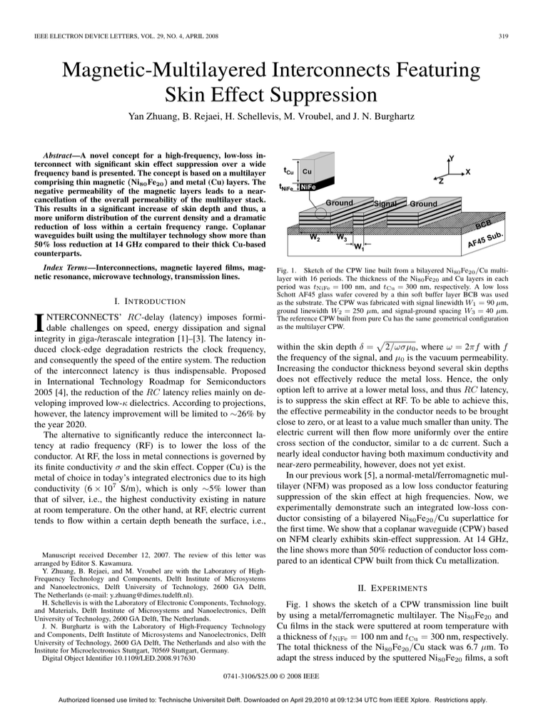
IEEE ELECTRON DEVICE LETTERS, VOL. 29, NO. 4, APRIL 2008 319 Magnetic-Multilayered Interconnects Featuring Skin Effect Suppression Yan Zhuang, B. Rejaei, H. Schellevis, M. Vroubel, and J. N. Burghartz Abstract—A novel concept for a high-frequency, low-loss interconnect with significant skin effect suppression over a wide frequency band is presented. The concept is based on a multilayer comprising thin magnetic (Ni80 Fe20 ) and metal (Cu) layers. The negative permeability of the magnetic layers leads to a nearcancellation of the overall permeability of the multilayer stack. This results in a significant increase of skin depth and thus, a more uniform distribution of the current density and a dramatic reduction of loss within a certain frequency range. Coplanar waveguides built using the multilayer technology show more than 50% loss reduction at 14 GHz compared to their thick Cu-based counterparts. Index Terms—Interconnections, magnetic layered films, magnetic resonance, microwave technology, transmission lines. I. I NTRODUCTION I NTERCONNECTS’ RC-delay (latency) imposes formidable challenges on speed, energy dissipation and signal integrity in giga-/terascale integration [1]–[3]. The latency induced clock-edge degradation restricts the clock frequency, and consequently the speed of the entire system. The reduction of the interconnect latency is thus indispensable. Proposed in International Technology Roadmap for Semiconductors 2005 [4], the reduction of the RC latency relies mainly on developing improved low-κ dielectrics. According to projections, however, the latency improvement will be limited to ∼26% by the year 2020. The alternative to significantly reduce the interconnect latency at radio frequency (RF) is to lower the loss of the conductor. At RF, the loss in metal connections is governed by its finite conductivity σ and the skin effect. Copper (Cu) is the metal of choice in today’s integrated electronics due to its high conductivity (6 × 10⁷ S/m), which is only ∼5% lower than that of silver, i.e., the highest conductivity existing in nature at room temperature. On the other hand, at RF, electric current tends to flow within a certain depth beneath the surface, i.e., Manuscript received December 12, 2007. The review of this letter was arranged by Editor S. Kawamura. Y. Zhuang, B. Rejaei, and M. Vroubel are with the Laboratory of HighFrequency Technology and Components, Delft Institute of Microsystems and Nanoelectronics, Delft University of Technology, 2600 GA Delft, The Netherlands (e-mail: y.zhuang@dimes.tudelft.nl). H. Schellevis is with the Laboratory of Electronic Components, Technology, and Materials, Delft Institute of Microsystems and Nanoelectronics, Delft University of Technology, 2600 GA Delft, The Netherlands. J. N. Burghartz is with the Laboratory of High-Frequency Technology and Components, Delft Institute of Microsystems and Nanoelectronics, Delft University of Technology, 2600 GA Delft, The Netherlands and also with the Institute for Microelectronics Stuttgart, 70569 Stuttgart, Germany. Digital Object Identifier 10.1109/LED.2008.917630 Fig. 1. Sketch of the CPW line built from a bilayered Ni80 Fe20 /Cu multilayer with 16 periods. The thickness of the Ni80 Fe20 and Cu layers in each period was tNiFe = 100 nm, and tCu = 300 nm, respectively. A low loss Schott AF45 glass wafer covered by a thin soft buffer layer BCB was used as the substrate. The CPW was fabricated with signal linewidth W1 = 90 µm, ground linewidth W2 = 250 µm, and signal-ground spacing W3 = 40 µm. The reference CPW built from pure Cu has the same geometrical configuration as the multilayer CPW. within the skin depth δ = 2/ωσµ0 , where ω = 2πf with f the frequency of the signal, and µ0 is the vacuum permeability. Increasing the conductor thickness beyond several skin depths does not effectively reduce the metal loss. Hence, the only option left to arrive at a lower metal loss, and thus RC latency, is to suppress the skin effect at RF. To be able to achieve this, the effective permeability in the conductor needs to be brought close to zero, or at least to a value much smaller than unity. The electric current will then flow more uniformly over the entire cross section of the conductor, similar to a dc current. Such a nearly ideal conductor having both maximum conductivity and near-zero permeability, however, does not yet exist. In our previous work [5], a normal-metal/ferromagnetic multilayer (NFM) was proposed as a low loss conductor featuring suppression of the skin effect at high frequencies. Now, we experimentally demonstrate such an integrated low-loss conductor consisting of a bilayered Ni80 Fe20 /Cu superlattice for the first time. We show that a coplanar waveguide (CPW) based on NFM clearly exhibits skin-effect suppression. At 14 GHz, the line shows more than 50% reduction of conductor loss compared to an identical CPW built from thick Cu metallization. II. E XPERIMENTS Fig. 1 shows the sketch of a CPW transmission line built by using a metal/ferromagnetic multilayer. The Ni80 Fe20 and Cu films in the stack were sputtered at room temperature with a thickness of tNiFe = 100 nm and tCu = 300 nm, respectively. The total thickness of the Ni80 Fe20 /Cu stack was 6.7 µm. To adapt the stress induced by the sputtered Ni80 Fe20 films, a soft 0741-3106/$25.00 © 2008 IEEE Authorized licensed use limited to: Technische Universiteit Delft. Downloaded on April 29,2010 at 09:12:34 UTC from IEEE Xplore. Restrictions apply. 320 IEEE ELECTRON DEVICE LETTERS, VOL. 29, NO. 4, APRIL 2008 Fig. 3. Quality factor of NFM- and Cu-CPW lines as a function of frequency. The quality factor was determined as Q = Im(γ)/2Re(γ) where γ is the complex propagation constant of the line. The maximum quality factor of the NFM line reaches 46 at 14 GHz, a ∼2-fold enhancement compared to the Cu reference. Fig. 2. Resistance per unit length of the NFM- and Cu-based CPW lines as a function of frequency. The inset shows the calculated effective skin depths of the NFM (δeff ) and Cu (δCu ) conductors. Near 10 GHz δeff ∼ δCu so that the conductor loss in the longitudinally magnetized NFM line becomes comparable to that of the Cu line. At 14 GHz δeff reaches its peak which is reflected as the dip in resistance per unit length of the NFM line. buffer layer of Benzocyclobutenes (BCB) was deposited between the Ni80 Fe20 /Cu stack and the nonalkaline Schott AF45 glass substrate. The electrical resistivity of the Cu and Ni80 Fe20 layers was found to be 1.8 and 16.3 µΩ · cm, respectively. A dc magnetic field of ∼10 mT was applied during the Ni80 Fe20 film deposition to induce magnetocrystalline anisotropy. The measured coercivities of the magnetic films were 2 and 5 mT, along the magnetic easy- and hard-axis, respectively. The multilayer was patterned by wet etching into a CPW line with a signal linewidth of 90 µm and signal-ground spacing of 40 µm. The length of the line was 2.5 mm. For comparison, an identical CPW line was built by using a uniform 6.7 µm-thick Cu layer on a BCB/glass substrate. S-parameter measurements were performed on an Agilent HP 8510 Vector Network Analyzer after LRM calibration and used to extract the electrical characteristics of the lines. An external dc magnetic field (HEXT ) of ∼10 mT was applied during the measurements along and perpendicular to the line to ensure saturation of the magnetic films in the desired direction. III. R ESULTS AND D ISCUSSION In Fig. 2, we have compared the resistance per unit length of the Cu line to that of the NFM line saturated in two different directions. While at low frequencies the longitudinally saturated (HEXT //z-axis) NFM line exhibited higher conductor loss compared to the Cu line, it showed significantly lower loss near 14 GHz. Compared to the Cu line, the conductor loss of the NFM line was more than 50% lower at this frequency, leading to a twice higher quality factor (Fig. 3). The other characteristic parameters of the CPW (inductance and capacitance per unit length) were found to be virtually unaffected by the NFM (results are not shown here). To qualitatively understand the frequency dependence of the conductor loss, we have computed the effective skin- √ depth δeff = 1/(Re jωµeff σeff ) in the NFM where σeff = (σNiFe tNiFe + σCu tCu )/t and µeff = µ0 (µ⊥ tNiFe + tCu )/t denote average conductivity, and permeability of the multilayer, respectively. Here, t = tNiFe + tCu , σNiFe and σCu represent the bulk conductivity of Ni80 Fe20 and Cu, respectively, and µ⊥ is the in-plane permeability of a Ni80 Fe20 film. The latter is a function of frequency and is given by µ⊥ = (ΩH + ωM )2 − ω 2 ΩH (ΩH + ωM ) − ω 2 where ΩH = γHa + jαω and ωM = γM where Ha is the static anisotropy field, M (∼1 T) is the saturation magnetization, γ is the gyrotropic constant, and α(∼ 0.01) is the Gilbert damping constant [6]. The result of the calculation is plotted as an inset in Fig. 2. For comparison, the skin depth in Copper (δCu ) is also shown. At frequencies below 10 GHz the effective skin depth in the multilayer is smaller than the skin depth in the Cu conductor. This is caused by the large (negative) real part of µ⊥ and, consequently, µeff . A smaller skin depth, together with a lower effective conductivity (σeff < σCu by ∼25%), explains the higher conductor loss observed in the multilayered CPW at low frequencies. With increasing frequency, however, the real part of µ⊥ becomes less negative [7] and δeff increases, eventually crossing δCu near 10 GHz. It is then not surprising that the NFM and Cu lines show nearly the same resistance per unit length near this frequency. At 14 GHz, the real part of µeff becomes zero and δeff reaches its peak value, causing the dip observed in the conductor loss of the NFM line. As the frequency is further increased, the real part of µeff becomes positive, and δeff becomes smaller again. Our calculation shows that the skin effect remains partially suppressed (δeff > δCu ) up to 28 GHz. (Note, that results beyond 16 GHz are affected by λ/4 resonance effects and insufficient measurement accuracy, therefore, are not shown here.) With the external magnetic field applied in the direction perpendicular to the line (H//x-axis), the dip in the conductor loss becomes much weaker and the result approaches to that of Authorized licensed use limited to: Technische Universiteit Delft. Downloaded on April 29,2010 at 09:12:34 UTC from IEEE Xplore. Restrictions apply. ZHUANG et al.: MAGNETIC-MULTILAYERED INTERCONNECTS FEATURING SKIN EFFECT SUPPRESSION the Cu CPW. This provides another proof of the magnetic origin of the conductor loss minimum in the multilayer CPW and can be understood as follows. The application of the external field along the x-axis aligns the static magnetization inside the Ni80 Fe20 layers with the magnetic field induced by the RF current. The magnetic layers then behave as normal metals, i.e., with unit permeability [6], and the overall behavior of the stack approaches that of a conventional metal. The frequency (fs ) at which the skin-effect suppression occurred depends on the ratio ξ = tCu /tNiFe [5]. Whereas a ratio of 3 led to fs = 14 GHz in our experiments, decreasing (increasing) ξ shifts fs to higher (lower) values, with an uplimit given by γ(M + Ha )/2π, i.e., the maximum frequency at which the magnetic layers still exhibit a negative permeability. Although the maximum operation frequency of Ni80 Fe20 -based multilayers is ∼28 GHz, much higher values can be achieved by using magnetic films with a high saturation magnetization. Calculations based on CoFe films (Ms ∼ 2.45 T) predict ∼2.6 times loss reduction at 60 GHz compared to Cu interconnects. Elaborate calculations such as in [5] show that even lower conductor loss can be achieved by using thinner metal and ferromagnetic layers and ferromagnetic layers with lower magnetic loss (smaller α). It is important to note that, in principle, on-chip multilayer wires do not require an external dc magnetic field. This is because the magnetic shape anisotropy due to the elongated shape of the magnetic films in the multilayer aligns the static magnetization parallel to the wire [8]. In our experiments, however, the excessive strain and stress in the multilayer deteriorated the magnetic alignment of the films, making the application of a bias field necessary. We believe that this problem can be addressed by using alternative deposition techniques (e.g., electroplating) to release the stress in the films. Alternatively, one can think of using self-biased ferromagnetic layers with an intrinsically high magnetocrystalline anisotropy. Finally, note that the application of multilayer conductors is not limited to 321 transmission line interconnects. Skin-effect suppression can, in principle, be employed to reduce the conductor loss of any RF component including spiral inductors and transformers. However, care has to be taken to align the static magnetization of the magnetic films inside the multilayered wires to lie in parallel with the wires’ direction. IV. C ONCLUSION We have reported a new concept of a low-loss conductor for RF interconnects, which allows for suppression of the skin effect. We showed that a CPW line built from a metal/magnetic multilayer exhibits more than 50% reduction of conductor loss compared to a conventional Cu line. We believe that this new concept provides a new means of advancing high-frequency and high-speed electronics. R EFERENCES [1] M. Morgen, E. T. Ryan, J. H. Zhao, C. Hu, T. H. Cho, and P. S. Ho, “Low dielectric constant materials for ULSI interconnects,” Annu. Rev. Mater. Sci., vol. 30, pp. 645–680, 2000. [2] R. Rosenberg, D. C. Edelstein, C. K. Hu, and K. P. Rodbell, “Copper metallization for high performance silicon technology,” Annu. Rev. Mater. Sci., vol. 30, pp. 229–262, 2000. [3] J. D. Meindl, Q. Chen, and J. A. Davis, “Limits on silicon nanoelectronics for terascale integration,” Science, vol. 293, no. 5537, pp. 2044–2048, 2001. [4] International Technology Roadmap for Semiconductors, 2005. [Online]. Available: http://public.itrs.net/ [5] B. Rejaei and M. Vroubel, “Suppression of skin-effect in metal/ ferromagnet superlattice conductors,” J. Appl. Phys., vol. 96, no. 11, pp. 6863–6868, Dec. 2004. [6] A. G. Gurevich and G. A. Melkov, Magnetization Oscillations and Waves. New York: CRC Press, 1996. [7] M. Vroubel, Y. Zhuang, B. Rejaei, and J. N. Burghartz, “Investigation of microstrips with NiFe magnetic thin film (II): Modeling,” Trans. Magn. Soc. Jpn., vol. 26, no. 12, pp. 371–376, 2002. [8] Y. Zhuang, M. Vroubel, B. Rejaei, J. N. Burghartz, and K. Attenborough, “Shape-induced ultrahigh magnetic anisotropy and ferromagnetic resonance frequency of micropatterned thin Permalloy films,” J. Appl. Phys., vol. 99, no. 8, pp. 08C705/1–08C705/3, 2006. Authorized licensed use limited to: Technische Universiteit Delft. Downloaded on April 29,2010 at 09:12:34 UTC from IEEE Xplore. Restrictions apply.
