CYStech Electronics Corp.
Spec. No. : C338S2
Issued Date : 2009.04.03
Revised Date : 2016.06.01
Page No. : 1/6
1.0Amp. Surface Mount Schottky Barrier Diodes
CSOD5817-5819S2
Features
For surface mounted applications.
For use in low voltage, high frequency inverters, free wheeling, and polarity protection applications
Plastic material used carries Underwriters Laboratory Flammability Classification 94V-0
Low leakage current
High surge capability
High temperature soldering: 250C/10 seconds at terminals
Exceeds environmental standards of MIL-S-19500/228
RoHS compliant package
Mechanical Data
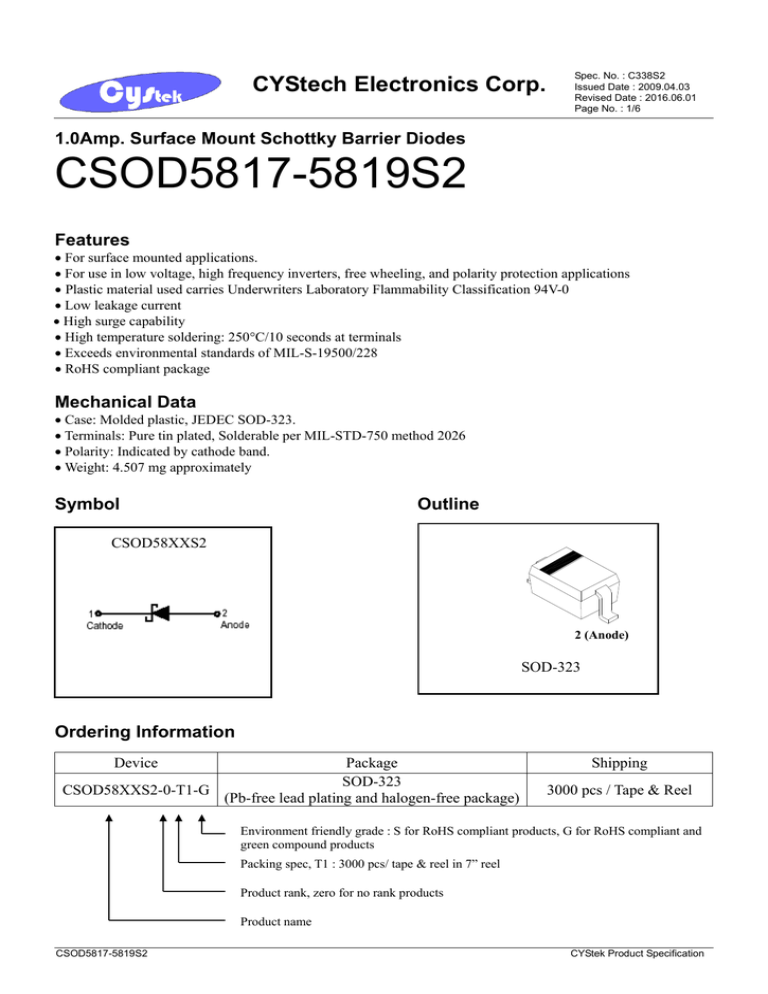
Case: Molded plastic, JEDEC SOD-323.
Terminals: Pure tin plated, Solderable per MIL-STD-750 method 2026
Polarity: Indicated by cathode band.
Weight: 4.507 mg approximately
Symbol
Outline
CSOD58XXS2
2 (Anode)
SOD-323
Ordering Information
Device
Package
SOD-323
CSOD58XXS2-0-T1-G
(Pb-free lead plating and halogen-free package)
Shipping
3000 pcs / Tape & Reel
Environment friendly grade : S for RoHS compliant products, G for RoHS compliant and
green compound products
Packing spec, T1 : 3000 pcs/ tape & reel in 7” reel
Product rank, zero for no rank products
Product name
CSOD5817-5819S2
CYStek Product Specification
CYStech Electronics Corp.
Spec. No. : C338S2
Issued Date : 2009.04.03
Revised Date : 2016.06.01
Page No. : 2/6
Maximum Ratings and Electrical Characteristics
(Rating at 25C ambient temperature unless otherwise specified. )
Parameter
Repetitive peak reverse voltage
Maximum RMS voltage
Maximum DC blocking voltage
Maximum instantaneous
forward voltage, IF=1A (Note 1)
Average forward rectified current
Peak forward surge current @8.3ms single
half sine wave superimposed on rated load
(JEDEC method)
Maximum DC reverse current
VR=VRRM,TJ=25℃(Note 1)
Maximum thermal resistance, Junction to
ambient
Power Dissipation @ TA=25°C
Diode junction capacitance @ f=1MHz and
applied 4V reverse voltage
Storage temperature range
Operating temperature range
VRRM
VRMS
VR
5817
20
14
20
Type
5818
30
21
30
5819
40
28
40
VF
0.45
0.55
0.6
Symbol
Units
V
V
V
V
IO
1
A
IFSM
10
A
IR
1
Rth,JA
500(typ)
℃/W
PD
250
mW
CD
120 (max)
pF
Tstg
TJ
-65 ~ +150
-50 ~ +150
℃
℃
mA
Notes : 1.Pulse test, pulse width=300μsec, 2% duty cycle
Recommended Footprint
mm
inch
CSOD5817-5819S2
CYStek Product Specification
CYStech Electronics Corp.
Spec. No. : C338S2
Issued Date : 2009.04.03
Revised Date : 2016.06.01
Page No. : 3/6
Characteristic Curves
CSOD5817-5819S2
CYStek Product Specification
CYStech Electronics Corp.
Spec. No. : C338S2
Issued Date : 2009.04.03
Revised Date : 2016.06.01
Page No. : 4/6
Reel Dimension
Carrier Tape Dimension
CSOD5817-5819S2
CYStek Product Specification
CYStech Electronics Corp.
Spec. No. : C338S2
Issued Date : 2009.04.03
Revised Date : 2016.06.01
Page No. : 5/6
Recommended wave soldering condition
Product
Pb-free devices
Peak Temperature
260 +0/-5 C
Soldering Time
5 +1/-1 seconds
Recommended temperature profile for IR reflow
Profile feature
Average ramp-up rate
(Tsmax to Tp)
Preheat
−Temperature Min(TS min)
−Temperature Max(TS max)
−Time(ts min to ts max)
Time maintained above:
−Temperature (TL)
− Time (tL)
Peak Temperature(TP)
Time within 5C of actual peak
temperature(tp)
Ramp down rate
Time 25 C to peak
temperature
Sn-Pb eutectic Assembly
Pb-free Assembly
3C/second max.
3C/second max.
100C
150C
60-120 seconds
150C
200C
60-180 seconds
183C
60-150 seconds
240 +0/-5 C
217C
60-150 seconds
260 +0/-5 C
10-30 seconds
20-40 seconds
6C/second max.
6C/second max.
6 minutes max.
8 minutes max.
Note : All temperatures refer to topside of the package, measured on the package body surface.
CSOD5817-5819S2
CYStek Product Specification
CYStech Electronics Corp.
Spec. No. : C338S2
Issued Date : 2009.04.03
Revised Date : 2016.06.01
Page No. : 6/6
SOD-323 Dimension
Marking:
K
A
XX
5H
2
1
B
D
Style: Pin 1.Cathode 2.Anode
J
H
E
C
2-Lead SOD-323 Plastic
Surface Mounted Package
CYStek Package Code: S2
Type
CSOD5817S2
CSOD5818S2
CSOD5819S2
Inches
Min.
Max.
0.0630 0.0709
0.0453 0.0531
0.0315 0.0394
0.0098 0.0157
DIM
A
B
C
D
Millimeters
Min.
Max.
1.60
1.80
1.15
1.35
0.80
1.00
0.25
0.40
DIM
E
H
J
K
Marking Code
SJ
SK
SL
Inches
Min.
Max.
0.0060
0.0000 0.0040
0.0035 0.0070
0.0906 0.1063
Millimeters
Min.
Max.
0.15
0.00
0.10
0.089
0.177
2.30
2.70
Notes: 1.Controlling dimension : millimeters.
2.Lead thickness specified per L/F drawing with solder plating.
3.If there is any question with packing specification or packing method, please contact your local CYStek sales office.
Material:
Lead: Pure tin plated.
Mold Compound: Epoxy resin family, flammability solid burning class: UL94V-0.
Important Notice:
All rights are reserved. Reproduction in whole or in part is prohibited without the prior written approval of CYStek.
CYStek reserves the right to make changes to its products without notice.
CYStek semiconductor products are not warranted to be suitable for use in Life-Support Applications, or systems.
CYStek assumes no liability for any consequence of customer product design, infringement of patents, or application assistance.
CSOD5817-5819S2
CYStek Product Specification
