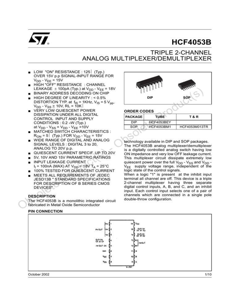
HCF4053B
TRIPLE 2-CHANNEL
ANALOG MULTIPLEXER/DEMULTIPLEXER
■
■
■
■
■
■
■
■
■
■
■
■
LOW "ON" RESISTANCE : 125Ω (Typ.)
OVER 15V p.p SIGNAL-INPUT RANGE FOR
VDD - VEE = 15V
HIGH "OFF" RESISTANCE : CHANNEL
LEAKAGE ± 100pA (Typ.) at VDD - VEE = 18V
BINARY ADDRESS DECODING ON CHIP
HIGH DEGREE OF LINEARITY : < 0.5%
DISTORTION TYP. at fIS = 1KHz, VIS = 5 Vpp,
VDD - VSS > 10V, RL = 10KΩ
VERY LOW QUIESCENT POWER
DISSIPATION UNDER ALL DIGITAL
CONTROL INPUT AND SUPPLY
CONDITIONS : 0.2 µW (Typ.)
at VDD - VSS = VDD - VEE =10V
MATCHED SWITCH CHARACTERISTICS :
RON = 5Ω (Typ.) FOR VDD - VEE = 15V
WIDE RANGE OF DIGITAL AND ANALOG
SIGNAL LEVELS : DIGITAL 3 to 20,
ANALOG TO 20V p.p.
QUIESCENT CURRENT SPECIF. UP TO 20V
5V, 10V AND 15V PARAMETRIC RATINGS
INPUT LEAKAGE CURRENT
II = 100nA (MAX) AT VDD = 18V TA = 25°C
100% TESTED FOR QUIESCENT CURRENT
MEETS ALL REQUIREMENTS OF JEDEC
JESD13B " STANDARD SPECIFICATIONS
FOR DESCRIPTION OF B SERIES CMOS
DEVICES"
)
(s
t
c
u
d
o
r
P
e
t
e
l
o
s
b
O
DESCRIPTION
The HCF4053B is a monolithic integrated circuit
fabricated in Metal Oxide Semiconductor
)
s
(
ct
DIP
SOP
PACKAGE
TUBE
t
e
l
o
DIP
SOP
u
d
o
r
P
e
ORDER CODES
HCF4053BEY
HCF4053BM1
T&R
HCF4053M013TR
s
b
O
technology available in DIP and SOP packages.
The HCF4053B analog multiplexer/demultiplexer
is a digitally controlled analog switch having low
ON impedance and very low OFF leakage current.
This multiplexer circuit dissipate extremely low
quiescent power over the full VDD - VSS and VDD VEE supply voltage range, independent of the
logic state of the control signals.
When a logic "1" is present at the inhibit input
terminal all channel are off. This device is a triple
2-channel multiplexer having three separate
digital control inputs, A, B, and C, and an inhibit
input. Each control input selects one of a pair of
channels which are connected in a single pole
double-throw configuration.
PIN CONNECTION
October 2002
1/10
HCF4053B
INPUT EQUIVALENT CIRCUIT
PIN DESCRIPTION
PIN No
SYMBOL
11, 10, 9
6
12, 13, 2, 1,
5, 3
14
15
4
A, B, C
INH
NAME AND FUNCTION
IN/OUT
Binary Control Inputs
Inhibit Inputs
ax,ay,bx,by,cx,cy Input/
Output
ax or ay
bx or by
cx or cy
7
OUT/IN
OUT/IN
OUT/IN
VEE
8
VSS
Negative Supply Voltage
16
VDD
Positive Supply Voltage
Supply Voltage
u
d
o
TRUTH TABLE
INHIBIT
C or B or A
0
0
1
0
1
X
FUNCTIONAL DIAGRAM
)
(s
t
c
u
d
o
r
P
e
t
e
l
o
s
b
O
2/10
r
P
e
t
e
l
o
X : Don’t Care
s
b
O
)
s
(
ct
ax or bx or cx
ay or by or cy
NONE
HCF4053B
ABSOLUTE MAXIMUM RATINGS
Symbol
VDD
Parameter
Value
Supply Voltage
VI
DC Input Voltage
II
DC Input Current
Unit
-0.5 to +22
V
-0.5 to VDD + 0.5
± 10
V
mA
500 (*)
100
mW
mW
Top
Power Dissipation per Package
Power Dissipation per Output Transistor
Operating Temperature
-55 to +125
°C
Tstg
Storage Temperature
-65 to +150
°C
PD
Absolute Maximum Ratings are those values beyond which damage to the device may occur. Functional operation under these conditions is
not implied.
All voltage values are referred to VSS pin voltage.
(*) 500mW at 65 °C; derate to 300mW by 10mW/°C from 65°C to 85°C
)
s
(
ct
u
d
o
RECOMMENDED OPERATING CONDITIONS
Symbol
VDD
Parameter
Supply Voltage
VI
Input Voltage
Top
Operating Temperature
e
t
e
ol
)
(s
Pr
Value
Unit
3 to 20
V
0 to VDD
V
-55 to 125
°C
s
b
O
t
c
u
d
o
r
P
e
t
e
l
o
s
b
O
3/10
HCF4053B
DC SPECIFICATIONS
Test Condition
Symbol
IL
Parameter
OFF*
OFF*
Resistance ∆RON
(between any 2 of
4 switches)
Input Capacitance
CO
Output
Capacitance
CIO
Feed through
l
o
s
ete
b
O
CI
5
10
20
100
150
300
600
3000
150
300
600
3000
µA
470
180
125
10
10
5
±0.1
1050
400
280
1200
520
360
1200
520
360
Ω
e
t
e
ol
0
0
0
0
0
0
18
o
r
P
Input Leakage
Current
Input Capacitance
0.04
0.04
0.04
0.08
0 < VI <
VDD
)-
-5
s
(
t
c
du
Input High Voltage
5
10
15
20
0
= VDD
thru
1KΩ
VEE = VSS
RL = 1KΩ
to VSS
IIS < 2µA
(on all OFF
channels)
VI = 0/18V
Min.
s
b
O
5
±0.1
100
Min.
Max.
Min.
Max.
)
s
(
t
c
u
d
o
r
P
100
Ω
1000
1000
nA
1000
1000
nA
5
pF
9
0.2
5
10
15
5
10
15
1.5
3
4
3.5
7
11
18
* Determined by minimum feasible leakage measurement for automating testing.
4/10
-40 to 85°C -55 to 125°C Unit
Max.
0
-5
TA = 25°C
Typ.
5
10
15
5
10
15
18
CONTROL (Address or Inhibit)
Input Low Voltage
VIL
IIH, IIL
VDD
(V)
0 < VI <
VDD
Channel Leakage
Current (All
Channel OFF)
(COMMON O/I)
Channel Leakage
Current (Any
Channel OFF)
CI
VIH
VSS
(V)
Quiescent Device
Current (all
switches ON or all
switches OFF)
SWITCH
RON Resistance
∆ON
VEE
(V)
VIS
(V)
Value
1.5
3
4
3.5
7
11
±10-3
±0.1
5
7.5
1.5
3
4
3.5
7
11
±1
V
V
±1
µA
pF
HCF4053B
DYNAMIC ELECTRICAL CHARACTERISTICS (Tamb = 25°C, CL = 50pF, all input square wave rise and
fall time = 20 ns )
Test Condition
Parameter
RL
(KΩ)
VEE
(V)
Propagation Delay
Time (signal input to
output)
Frequency Response
Channel "ON" (sine
wave input) at
20 log VO/VI = - 3dB
Feed through (all
channels OFF) at
20 log VO/VI = - 40dB
Frequency Signal
Crosstalk at
20 log VO/VI = -40dB
fI
(KHz)
1
= VSS
5(*)
1
= VSS
10
CONTROL (Address or Inhibit)
Propagation Delay:
0
Address to Signal
0
OUT (Channels ON
0
or OFF)
-5
Propagation Delay:
0
Inhibit to Signal OUT
0
1
(Channel turning ON)
0
-10
Propagation Delay:
0
Inhibit to Signal OUT
0
10
(Channel turning
0
OFF)
-10
1
)
s
(
ct
du
e
t
e
ol
o
r
P
s
b
O
Address or Inhibit to
Signal Crosstalk
0
2(*)
3(*)
5(*)
10 (1)
Min. Typ. Max.
5
10
15
30
15
11
10
5(*)
o
s
b
0
0
0
0
0
0
0
0
0
VO at Common
OUT/IN
VO at any
channel
VO at Common
OUT/IN
VO at any
channel
Between any 2
Sections (IN pin
2, OUT pin 14)
Between any 2
Sections (lN pin
15, OUT pin 14)
e
t
e
l
10
-O
Unit
VDD
(V)
10
5(*)
1
Sine Wave Distortion
= VSS
fIS = 1KHz Sine Wave
VSS
(V)
VDD
200
= VSS
VI
(V)
Value
MHz
)
s
(
ct
60
10
du
o
r
P
MHz
8
2.5
MHz
6
0.3
0.2
0.12
5
10
15
5
5
10
15
5
5
10
15
5
360
160
120
225
360
160
120
200
200
90
70
130
VC = VDD-VSS
(square wave)
ns
25
5
10
15
10
60
30
20
65
%
720
320
240
450
720
320
240
400
450
210
160
300
ns
ns
ns
mV
peak
(1) Both ends of channel.
* Peak to Peak voltage symmetrical about (VDD - VEE ) /2
5/10
HCF4053B
TYPICAL BIAS VOLTAGES
)
s
(
ct
u
d
o
r
P
e
The ADDRESS (digital-control inputs) and INHIBIT logic levels are : "0"=VSS and "1"=VDD. The analog signal (through the TG) may swing
from VEE to VDD
SPECIAL CONSIDERATIONS
Control of analog signals up to 20V peak to peak
can be achieved by digital signal amplitudes of 4.5
to 20V (if VDD - VSS = 3V, a VDD - VEE of up to 13V
can be controlled; for VDD - VEE level differences
above 13V, a VDD - VSS of at least 4.5V is
required. For example, if VDD = +5, VSS = 0, and
VEE = -13.5, analog signals from -13.5V to 4.5V
can be controlled by digital inputs of 0 to 4.5V. In
TEST CIRCUIT
)
(s
t
c
u
d
o
r
P
e
t
e
l
o
s
b
O
CL = 50pF or equivalent (includes jig and probe capacitance)
RL = 200KΩ
RT = ZOUT of pulse generator (typically 50Ω)
6/10
t
e
l
o
certain applications, the external load resistor
current may include both VDD and signal-line
components. To avoid drawing VDD current when
switch current flows into the transmission gate
inputs, the voltage drop across the bidirectional
switch must not exceed 0,8V (calculated from RON
values shown in DC SPECIFICATIONS). No VDD
current will flow through RL if the switch current
flows into leads 4, 14 and 15.
s
b
O
HCF4053B
WAVEFORM 1 : CHANNEL BEING TURNED ON (RL = 1KΩ, f=1MHz; 50% duty cycle)
)
s
(
ct
u
d
o
r
P
e
t
e
l
o
s
b
O
WAVEFORM 2 : CHANNEL BEING TURNED OFF (RL = 1KΩ, f=1MHz; 50% duty cycle)
)
(s
t
c
u
d
o
r
P
e
t
e
l
o
s
b
O
7/10
HCF4053B
Plastic DIP-16 (0.25) MECHANICAL DATA
mm.
inch
DIM.
MIN.
a1
0.51
B
0.77
TYP
MAX.
MIN.
TYP.
MAX.
0.020
1.65
0.030
0.065
b
0.5
0.020
b1
0.25
0.010
D
)
s
(
ct
20
E
8.5
e
2.54
e3
17.78
u
d
o
0.335
7.1
I
5.1
s
(
t
c
1.27
e
t
e
ol
bs
O
)
3.3
Z
Pr
0.100
F
L
0.787
0.700
0.280
0.201
0.130
0.050
u
d
o
r
P
e
t
e
l
o
s
b
O
P001C
8/10
HCF4053B
SO-16 MECHANICAL DATA
mm.
DIM.
MIN.
TYP
A
inch
MAX.
MIN.
TYP.
a1
1.75
MAX.
0.1
0.068
0.2
a2
0.003
0.007
1.65
0.064
b
0.35
0.46
0.013
0.018
b1
0.19
0.25
0.007
0.010
C
0.5
c1
45˚ (typ.)
D
9.8
E
5.8
)
s
(
ct
0.019
e
1.27
e3
8.89
10
0.385
6.2
0.228
4.0
G
4.6
L
0.5
s
b
O
5.3
1.27
)
(s
ete
ol
3.8
S
Pr
0.393
0.244
0.050
F
M
u
d
o
0.62
0.350
0.149
0.157
0.181
0.208
0.019
0.050
0.024
8 ˚ (max.)
t
c
u
d
o
r
P
e
t
e
l
o
s
b
O
PO13H
9/10
HCF4053B
)
s
(
ct
u
d
o
r
P
e
t
e
l
o
)
(s
s
b
O
t
c
u
d
o
r
P
e
t
e
l
o
s
b
O
Information furnished is believed to be accurate and reliable. However, STMicroelectronics assumes no responsibility for the
consequences of use of such information nor for any infringement of patents or other rights of third parties which may result from
its use. No license is granted by implication or otherwise under any patent or patent rights of STMicroelectronics. Specifications
mentioned in this publication are subject to change without notice. This publication supersedes and replaces all information
previously supplied. STMicroelectronics products are not authorized for use as critical components in life support devices or
systems without express written approval of STMicroelectronics.
© The ST logo is a registered trademark of STMicroelectronics
© 2002 STMicroelectronics - Printed in Italy - All Rights Reserved
STMicroelectronics GROUP OF COMPANIES
Australia - Brazil - Canada - China - Finland - France - Germany - Hong Kong - India - Israel - Italy - Japan - Malaysia - Malta - Morocco
Singapore - Spain - Sweden - Switzerland - United Kingdom - United States.
© http://www.st.com
10/10
