Low Dose Rate Test Results of National Semiconductor`s ELDRS
advertisement

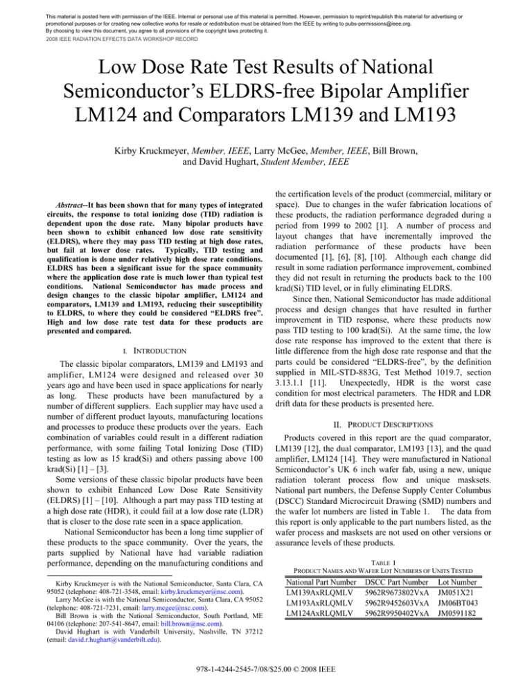
This material is posted here with permission of the IEEE. Internal or personal use of this material is permitted. However, permission to reprint/republish this material for advertising or promotional purposes or for creating new collective works for resale or redistribution must be obtained from the IEEE by writing to pubs-permissions@ieee.org. By choosing to view this document, you agree to all provisions of the copyright laws protecting it. 2008 IEEE RADIATION EFFECTS DATA WORKSHOP RECORD Low Dose Rate Test Results of National Semiconductor’s ELDRS-free Bipolar Amplifier LM124 and Comparators LM139 and LM193 Kirby Kruckmeyer, Member, IEEE, Larry McGee, Member, IEEE, Bill Brown, and David Hughart, Student Member, IEEE Abstract--It has been shown that for many types of integrated circuits, the response to total ionizing dose (TID) radiation is dependent upon the dose rate. Many bipolar products have been shown to exhibit enhanced low dose rate sensitivity (ELDRS), where they may pass TID testing at high dose rates, but fail at lower dose rates. Typically, TID testing and qualification is done under relatively high dose rate conditions. ELDRS has been a significant issue for the space community where the application dose rate is much lower than typical test conditions. National Semiconductor has made process and design changes to the classic bipolar amplifier, LM124 and comparators, LM139 and LM193, reducing their susceptibility to ELDRS, to where they could be considered “ELDRS free”. High and low dose rate test data for these products are presented and compared. I. INTRODUCTION The classic bipolar comparators, LM139 and LM193 and amplifier, LM124 were designed and released over 30 years ago and have been used in space applications for nearly as long. These products have been manufactured by a number of different suppliers. Each supplier may have used a number of different product layouts, manufacturing locations and processes to produce these products over the years. Each combination of variables could result in a different radiation performance, with some failing Total Ionizing Dose (TID) testing as low as 15 krad(Si) and others passing above 100 krad(Si) [1] – [3]. Some versions of these classic bipolar products have been shown to exhibit Enhanced Low Dose Rate Sensitivity (ELDRS) [1] – [10]. Although a part may pass TID testing at a high dose rate (HDR), it could fail at a low dose rate (LDR) that is closer to the dose rate seen in a space application. National Semiconductor has been a long time supplier of these products to the space community. Over the years, the parts supplied by National have had variable radiation performance, depending on the manufacturing conditions and the certification levels of the product (commercial, military or space). Due to changes in the wafer fabrication locations of these products, the radiation performance degraded during a period from 1999 to 2002 [1]. A number of process and layout changes that have incrementally improved the radiation performance of these products have been documented [1], [6], [8], [10]. Although each change did result in some radiation performance improvement, combined they did not result in returning the products back to the 100 krad(Si) TID level, or in fully eliminating ELDRS. Since then, National Semiconductor has made additional process and design changes that have resulted in further improvement in TID response, where these products now pass TID testing to 100 krad(Si). At the same time, the low dose rate response has improved to the extent that there is little difference from the high dose rate response and that the parts could be considered “ELDRS-free”, by the definition supplied in MIL-STD-883G, Test Method 1019.7, section 3.13.1.1 [11]. Unexpectedly, HDR is the worst case condition for most electrical parameters. The HDR and LDR drift data for these products is presented here. II. PRODUCT DESCRIPTIONS Products covered in this report are the quad comparator, LM139 [12], the dual comparator, LM193 [13], and the quad amplifier, LM124 [14]. They were manufactured in National Semiconductor’s UK 6 inch wafer fab, using a new, unique radiation tolerant process flow and unique masksets. National part numbers, the Defense Supply Center Columbus (DSCC) Standard Microcircuit Drawing (SMD) numbers and the wafer lot numbers are listed in Table 1. The data from this report is only applicable to the part numbers listed, as the wafer process and masksets are not used on other versions or assurance levels of these products. TABLE I PRODUCT NAMES AND WAFER LOT NUMBERS OF UNITS TESTED Kirby Kruckmeyer is with the National Semiconductor, Santa Clara, CA 95052 (telephone: 408-721-3548, email: kirby.kruckmeyer@nsc.com). Larry McGee is with the National Semiconductor, Santa Clara, CA 95052 (telephone: 408-721-7231, email: larry.mcgee@nsc.com). Bill Brown is with the National Semiconductor, South Portland, ME 04106 (telephone: 207-541-8647, email: bill.brown@nsc.com). David Hughart is with Vanderbilt University, Nashville, TN 37212 (email: david.r.hughart@vanderbilt.edu). 978-1-4244-2545-7/08/$25.00 © 2008 IEEE III. TEST METHOD All units tested were assembled in the ceramic Dual Inline Package (DIP) and processed through the class V flow in MIL-PRF-38535 [15]. Radiation testing was done using the ELDRS characterization in MIL-STD-883, Test Method 1019.7, section 3.13.1.1 as a guide. A four way split was run with units biased and unbiased during irradiation at LDR and HDR. The conditions used for irradiation and the number of units analyzed for each product type are shown in Table II. For the LM124 and the LM139, the units came from one wafer each. For the LM193, the units came from two different wafers. TABLE II TEST CONDITIONS FOR THE FOUR WAY SPLIT The HDR irradiation was done between 37 to 45 rad(Si)/s at National Semiconductor’s radiation facility in South Portland, Maine. The LDR irradiation was done at 10 mrad(Si)/s at White Sands Missile Range. The unbiased units had all leads tied to ground during irradiation. For the biased units, on the LM193 and LM139, the supply was connected to 28 V, the inverting inputs to 6.4 V, the noninverting inputs to 10 V and the outputs to ground. For the LM124 the supplies were connected to +15 and -15 V, the inputs were tied together through a 30 kohm resistor, and the outputs and inputs were ganged together through 10 kohm resistors and connected to ground. Electrical testing was done with an LTX77 test system at National Semiconductor’s South Portland radiation facility. All datasheet and SMD parameters were tested. For the HDR legs testing was done at 0, 3, 10, 30, 50 and 100 krad(Si) levels. The LDR legs were pulled at close to the same levels, but not always exactly at those levels. For instance, on the LM139, the 50 krad(Si) level was actually tested at 48 krad(Si). For all three products, the LDR testing was taken to 102 krad(Si). For the HDR legs, electrical testing was completed within an hour of being removed from the gamma radiation. The LDR legs were shipped overnight from the test facility at WSMR to National for testing, and shipped back overnight to WSMR to resume irradiation. Testing time limits were in accordance with MIL-STD-883G, TM1019.7. IV. RESULTS All legs passed TID testing to a radiation level of 100 krad(Si) with all parameters inside the post irradiation limits on the datasheets and SMDs. The products can be considered “ELDRS free” based on the definition in MIL-STD-883G, Test Method 1019.7, section 13.3.1.1. No parameters have an LDR drift that is 1.5 times greater than the HDR drift and have the post irradiation values outside the pre irradiation limits [11]. The average parametric drift and the standard deviation of the drift for each test for the three products are listed in Tables III, IV and V. The drift was calculated from the 0 krad test point to the maximum test point, 100 krad(Si) for HDR and 102 krad(Si) for LDR. The data is shown for the worst case channel that had the highest amount of drift for most tests. For the LM139 and LM193, the worst case was channel 1, while for the LM124 it was channel 4. V. DISCUSSION OF THE RESULTS The worst case test conditions resulting in the highest drift through irradiation varied from parameter to parameter. In most cases, HDR resulted in higher drift than LDR. The impact of biasing during irradiation varied from parameter to parameter and part to part. Except for the input offset current on the LM124, there was not much channel to channel variation in TID radiation response for any of the products. The average parametric readings at each of the radiation test points for select tests are plotted in Figs. 1 through 19. In some cases the results of the four different radiation conditions are compared, and in other cases, the different channels are compared for one radiation condition. Unless otherwise noted, the scale range of the y axis is the pre irradiation test limits. TABLE III DRIFT RESULTS OF SELECTED PARAMETERS FOR LM193 CHANNEL 1 111 TABLE IV DRIFT RESULTS OF SELECTED PARAMETERS FOR LM139 CHANNEL 1 TABLE V DRIFT RESULTS OF SELECTED PARAMETERS FOR LM124 CHANNEL 4 A. LM193 The parameters with the highest sensitivity to radiation are the input offset voltage, input bias current, and response time, which are plotted in Figs. 1 through 3 respectively. The input offset current and supply current are fairly radiation hard and are plotted in Figs. 4 and 5 respectively. The data is all for channel 1. Little variation was seen between channel 1 and 2. Fig. 1 LM193 input offset voltage vs. radiation exposure for channel 1, with Vcc = 5 V and Vcm = 0 V. The y axis range is the pre irradiation limits. The HDR drifts are usually larger, sometimes significantly larger, than the LDR drifts, as can be seen from Table 3 and Figs. 1-3. For most tests, the unbiased condition resulted in more drift than when the parts were biased. The major exception is response time, where the biased conditions were worst case (Fig. 3). Fig. 2 LM193 input bias current vs. radiation exposure for channel 1 with Vcc = 5 V and Vcm = 0 V. The y axis range is the pre irradiation limits. 112 For input bias current, under HDR, the direction of the drift was in opposite directions depending on whether the part was biased, being in the negative direction when the units were biased, and the positive direction when unbiased during irradiation (Fig. 1). There was very little movement in this parameter under LDR irradiation. B. LM139 The parameters most sensitive to TID radiation are the input offset voltage, input bias current, and response time. They are plotted in Figs. 6 - 8 respectively. The input offset current shows small responses to the radiation (Fig. 9) and the supply current remains largely unchanged (Fig. 10). Fig. 3 LM193 response time vs. radiation exposure for channel 1 with Vcc = 5 V and Vod = 50 mV. The pre irradiation limit is 0.8 µs and the post irradiation limit is 1.0 µs. Fig. 6 LM139 input offset voltage vs. radiation exposure for channel 1. with Vcc = 30V and Vcm = 0 V. The y axis range is the pre irradiation limits. Fig. 4 LM193 input offset current vs. radiation exposure for channel 1, with Vcc = 5 V and Vcm = 0 V. The y axis range is pre irradiation limits. Fig. 5 LM193 supply current vs. radiation exposure with Vcc = 5 V. The y axis range is the pre irradiation limits. Fig. 7 LM139 input bias current vs. radiation exposure for channel 1, with Vcc = 5 V and Vcm = 0 V. The y axis range is pre irradiation limits. Fig. 8 LM139 response time vs. radiation exposure for channel 1 with Vcc = 5 V and Vod = 5 mV The y axis range is pre irradiation limits. 113 parameter and dose rate, but the biased condition tended to be the worst case for many of the tests. Fig. 9 LM139 input offset current vs. radiation exposure for channel 1 with Vcc = 5 V and Vcm = 0 V. The y axis range is pre irradiation limits. Fig. 12 LM139 response time vs. radiation exposure for all channels when biased at LDR with Vcc = 5 V and Vod = 5 mV. The y-axis range is the pre irradiation limits. Fig. 10 LM139 supply current vs. radiation exposure with Vcc = 30 V. The y axis range is the pre irradiation limits. Fig. 13 LM139 input offset current vs. radiation exposure for all channels when unbiased at LDR with Vcc = 5 V and Vcm = 0 V The y axis range is the pre irradiation limits. The input offset voltage parameter showed multiple types of variation. In Fig. 6, the LDR biased case shows a brief upward spike at 13 krad and then a sharp drop followed by steady degradation. This spike appears on every channel when testing biased devices at LDR conditions (Fig. 11). Similar to the LM193, the LM139 input offset voltage drift under HDR irradiation is dependent on biasing conditions, with a negative drift seen with the parts biased and a positive drift with the parts unbiased (Table VI). Fig. 11 LM139 input offset voltage vs. radiation exposure for all channels when biased at LDR with Vcc = 30 V and Vcm = 0 V. The y axis range is the pre irradiation limits. TABLE VI DRIFT RESULTS FOR INPUT OFFSET VOLTAGE FOR LM139 ALL CHANNELS In most cases the LDR drift through irradiation was the same, or sometimes significantly less than the HDR drift. In the few cases where LDR drift was higher than the HDR drift, the difference was within the standard deviation of the drift. The impact of the biasing condition varied by 114 Previous versions of the LM139 were reported to show wide channel to channel variations in TID response. For instance, on one older version of the LM139, the channel 1 input offset voltage would shift by -15 mV at 30 krad(Si), while the input offset voltage on the other three channels would shift by less than 5 mV out to 100 krad(Si) [1]. For this new ELDRS-free version of the LM139, there is some channel to channel variation in TID response, but it is not significant (Figs. 11 – 13). C. LM124 The parameter showing the most sensitivity to TID radiation was the input bias current, which is plotted in Fig. 14. The supply current, voltage gain, and input offset voltage also showed some sensitivity (Figs. 15 - 17). The input offset current does not show much response to radiation (Fig. 18). There was not much difference in TID radiation response between the LDR and HDR conditions. Generally, the biased condition was the worst case. Fig. 16 LM124 voltage gain vs. radiation exposure for channel 4 with Vo = 5 V to 20V, Vcc = 30 V, and RL=2kΩ. The y axis range is the pre irradiation limits. Fig. 17 LM124 input offset voltage vs. radiation exposure for channel 4 with +Vcc = 2.5 V, -Vcc = -2.5 V, and Vcm = 1.1 V. The y axis range is the pre irradiation limits. Fig. 14 LM124 input bias current vs. radiation exposure for channel 4 with Vcc = 30 V and Vcm = -15 V. The pre irradiation limit is -50 nA and the post irradiation limit is -75 nA. Fig. 18 LM124 input offset current vs. radiation exposure for channel 4 with Vcc = 30 V and Vcm = -15 V. The y axis range is the pre irradiation limits. Fig. 15 LM124 supply current vs. radiation exposure with Vcc = 30 V. The y axis range is the pre irradiation limits. The only test with significant channel variation was the input offset current. Regardless of the biasing or dose rate conditions, channels 1 and 4 would always drift positively and channels 2 and 3 would always drift negatively. The cause for this may be that prior to irradiation channels 1 and 4 115 tend to have slightly positive offset currents and channels 2 and 3 tend to have near zero or slightly negative offset currents. During irradiation, a channel would drift in accordance with its initial offset current value. This channel divergence is not an isolated trend; it appears on other wafers tested in this wafer lot. The biased HDR case is shown in Fig. 19. 100 krad(Si). In most cases, the low dose rate drift is less than that for high dose rate. This is for the products designated “ELDRS-free” and is not applicable to other versions of these products. Biasing conditions during irradiation can have a variable impact TID response, with a biased condition being the worst case for some parameters and an unbiased condition being worst case for others. For some parameters, the drift over the radiation range is not monotonic, with the drift switching directions at some interim test point. Although other wafers and wafer lots of these products have been tested and have passed the low dose rate testing, this study does not comprehend lot to lot variations in TID response. For this reason, National continues to test and qualify each individual wafer under LDR, taking data at the interim radiation points as was done in this study. VII. REFERENCES [1] Fig. 19 LM124 input offset current vs. radiation exposure for all channels when biased at HDR with Vcc = 30 V and Vcm = -15 V. The pre irradiation limit is -10 nA to 10 nA. In general, the variation in drift from channel to channel was minor compared with unit to unit or wafer to wafer variation. Typically there was more variation in drift on units within a wafer than in the average wafer to wafer drift. Table VII shows the channel to channel, unit to unit and wafer to wafer standard deviations for the drift from 0 to 102 krad(Si) for LDR testing. In the Avg. Drift column is the average drift for channel 4 for the five units used in this study. These units came from the same wafer. The channel to channel drift standard deviation was calculated from the four channels of one unit. The unit to unit drift standard deviation was calculated for channel 4 for the 5 units tested from the one wafer used in this study. The wafer to wafer calculation is from the average drift for channel 4 from 5 units per wafer, from the one wafer used in this study and five other wafers from the same wafer lot. TABLE VII CHANNEL, UNIT AND WAFER DRIFT VARIATION VI. CONCLUSIONS The latest space versions of National Semiconductor’s bipolar amplifier, LM124 and comparators LM139 and LM193 do not exhibit ELDRS and are qualified to a TID of R. L. Pease, M. C. Maher, M. R. Shaneyfelt, M. W. Savage, P. Baker, J. Krieg, and T. L. Turflinger, “Total-dose hardening of a bipolarvoltage comparator,” IEEE Trans. Nucl. Sci., vol. 49, no. 6, pp. 31803184, Dec. 2002. [2] R. L. Pease, S. McClure, A. H. Johnson, J. Gorelick, T. L. Turflinger, M. Gehlhausen, J. Krieg, T. Carriere, M. Shaneyfelt, “An updated data compendium of enhanced low dose rate sensitive (ELDRS) bipolar integrated circuits,” 2001 IEEE Radiation Effects Data Workshop, pp. 127-133 [3] H. J. Barnaby, C. R. Criba, R. D. Schrimpf, D. M. Fleetwood, R. L. Pease, M. R. Shaneyfelt, T. Turflinger, J. F. Krieg, M. H. Maher, “Origins of total-dose response variability in linear bipolar microcircuits,” IEEE Trans. Nucl. Sci., Vol. 47, no. 6, pp. 2342-2348, Dec. 2000 [4] R. L. Pease, “Total ionizing dose effects in bipolar devices and circuits,” IEEE Trans. Nucl. Sci., Vol. 50, no. 3, June 2003 [5] L. Dusseau, M. F. Bernard, J. Boch, J. -R. Vaillé, F. Saigné, R. D. Schrimpf, E. Lorfèvre, and J. P. David, "Analysis of total-dose response of a bipolar voltage comparator combining radiation experiments and design data," IEEE Trans. Nucl. Sci., vol. 53, no. 4, pp. 1910-1916, Aug. 2006. [6] M. R. Shaneyfelt, J. R. Schwank, J. A. Felix, P. E. Dodd, D. M. Fleetwood, R. L. Pease, and M. C. Maher, ‘‘Annealing behavior of linear bipolar devices with enhanced low-dose-rate sensitivity,’’ IEEE Trans. Nucl. Sci., vol. 51, pp. 3172---3177, Dec. 2004. [7] R. L. Pease, G. Platteter, G. W. Dunham, J. E. Seiler, H. J. Barnaby, R. D. Schrimpf, M. R. Shaneyfelt, M. C. Maher, and R. N. Nowlin, ‘‘Characterization of enhanced low dose rate sensitivity (ELDRS) effects using gated lateral PNP transistor structures,’’ IEEE Trans. Nucl. Sci., vol. 51, no. 6, pp. 3773-3780, Dec. 2004. [8] M. R. Shaneyfelt, R. L. Pease, M. C. Maher, J. R. Schwank, S. Gupta, P. E. Dodd, and L. C. Riewe, ‘‘Passivation layers for reduced total dose effects and ELDRS in linear bipolar devices, IEEE Trans. Nucl. Sci., vol. 50, no. 6, pp. 1784-1790, Dec. 2003. [9] H. J. Barnaby, R. D. Schrimpf, R. L. Pease, P. Cole, T. Turflinger, J. Krieg, J. Titus, D. Emily, M. Gehlhausen, S. C. Witczak, M. C. Maher, and D. Van Nort, “Identification of degradation mechanisms in bipolar linear voltage comparator through correlation of transistor and circuit response,” IEEE Trans. Nucl. Sci., vol. 46, no. 6, pp. 1666-1673, Dec. 1999. [10] M. R. Shaneyfelt, R. L. Pease, J. R. Schwank, M. C. Maher, G. L. Hash, D. M. Fleetwood, P. E. Dodd, C. A. Reber, S. C. Witczak, L. C. Riewe, H. P. Hjalmarson, J. C. Banks, B. L. Doyle, and J. A. Knapp, “Impact of passivation layers on enhanced low-dose-rate sensitivity and pre-irradiation elevated-temperature stress effects in linear ICs,” IEEE Trans. Nucl. Sci., vol. 49, no. 6, pp. 3171-3179, Dec. 2002. [11] MIL-STD-883 Test Method Standard, Microcircuits, Department of Defense, Defense Supply Center Columbus, Columbus, OH, June18, 2004 http://www.dscc.dla.mil/Downloads/MilSpec/Docs/MIL-STD883/std883.pdf 116 [12] “LM139A/LM139QML Low Power Low Offset Voltage Quad Comparators,” April 2, 2008, National Semiconductor, Santa Clara, CA, http://cache.national.com/ds/LM/LM139A.pdf [13] “LM193A/LM193QML Low Power Low Offset Voltage Dual Comparators,” October, 2007, National Semiconductor, Santa Clara, CA, http://cache.national.com/ds/LM/LM193A.pdf [14] “LM124A/LM124QML Low Power Quad Operational Amplifiers,” June 2006, National Semiconductor, Santa Clara, CA, http://cache.national.com/ds/LM/LM124A.pdf [15] MIL-PRF-38535 Integrated Circuits (Microcircuits) Manufacturing, General Specification for, Department of Defense, Defense Supply Center Columbus, Columbus, OH, Mar 16, 2007 http://www.dscc.dla.mil/Downloads/MilSpec/Docs/MIL-PRF38535/prf38535.pdf 117


