AN1690, Alarm IC General Applications Overview

Freescale Semiconductor
Application Note
AN1690
Rev 4, 05/2005
Alarm IC General Applications Overview
by: Leticia Gomez and Diana Pelletier, Sensor Applications Engineering
Sensor Products, Systems and Applications Engineering
INTRODUCTION
The MC14600, an IC designed for alarm applications, is a versatile part that can easily be configured with a minimum number of external components to serve a wide range of alarm applications and circuit configurations. For example, the
MC14600 can be used in systems that detect pressure and temperature change, liquid levels, motion or intrusion. This application note presents considerations in interfacing external components to the MC14600 and an approach for configuring it with a latch.
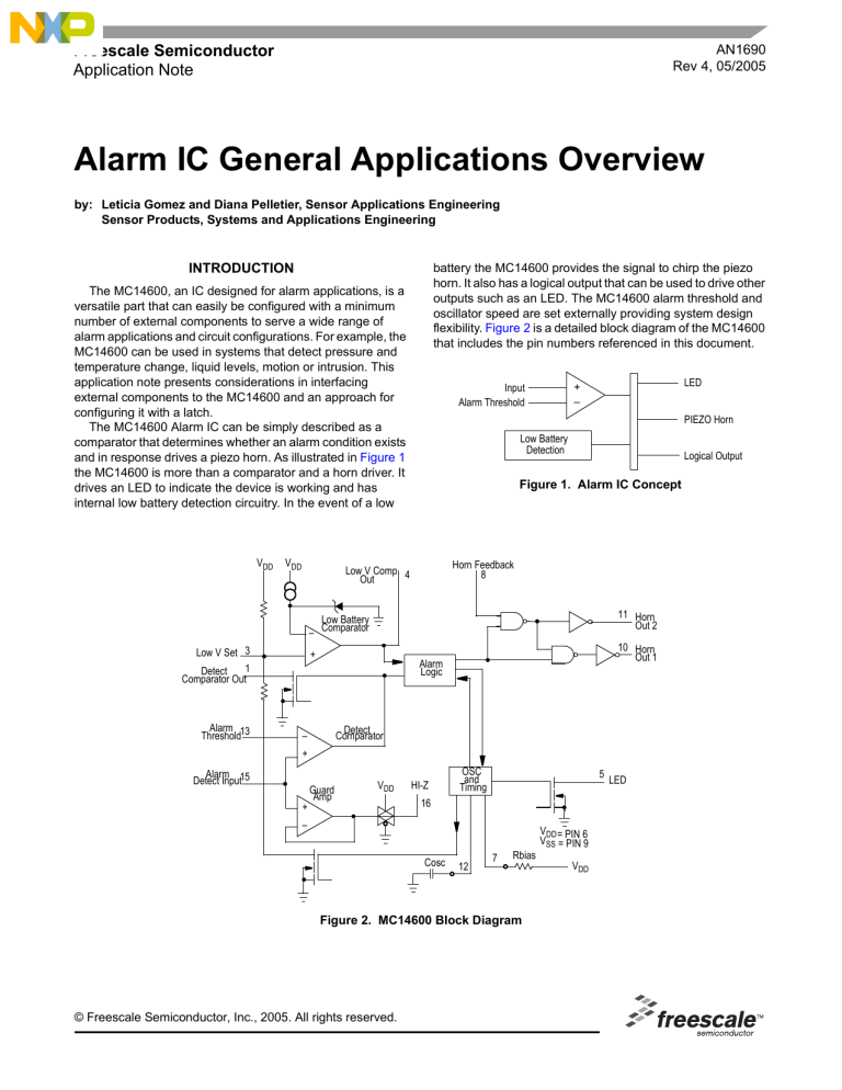
The MC14600 Alarm IC can be simply described as a comparator that determines whether an alarm condition exists and in response drives a piezo horn. As illustrated in
the MC14600 is more than a comparator and a horn driver. It drives an LED to indicate the device is working and has internal low battery detection circuitry. In the event of a low battery the MC14600 provides the signal to chirp the piezo horn. It also has a logical output that can be used to drive other outputs such as an LED. The MC14600 alarm threshold and oscillator speed are set externally providing system design
flexibility. Figure 2 is a detailed block diagram of the MC14600
that includes the pin numbers referenced in this document.
Input
Alarm Threshold
+
–
LED
PIEZO Horn
Low Battery
Detection
Figure 1. Alarm IC Concept
Logical Output
V
DD
V
DD
4
Horn Feedback
8
Low V Set 3
Comparator Out
1
–
+
11
10 Horn
Out 1
Alarm
15
–
+
+
–
V
DD
HI-Z
16
Cosc
12
7
Rbias
V
V
DD
SS
= PIN 6
= PIN 9
V
DD
5 LED
Figure 2. MC14600 Block Diagram
© Freescale Semiconductor, Inc., 2005. All rights reserved.
ALARM THRESHOLD ADJUSTMENTS
The alarm trigger point (alarm threshold) is set externally to any voltage level with a simple voltage divider connected to pin 13. For instance, to connect the Alarm IC to a sensor that has an output of 1.0 V during a no alarm condition and 4.0 V during an alarm condition, the alarm threshold voltage could be set to 3.0 V using a 2 M Ω and a 1 M Ω resistor connected between V
DD
and ground (See Figure 3 ). Pin 13 connects
internally to the negative input of the Detect Comparator.
Based on the input impedance of the Detect Comparator the maximum suggested total resistance for the threshold voltage divider is 10 M Ω .
V
DD
2M
PIN 13
1M
PIEZO HORN INTERFACE
The MC14600 contains on-board horn driver circuitry to drive three leaded piezo horns. A three leaded horn is considered self-driven, having a feedback pin that is connected to a closed loop oscillation circuit. The MC14600 uses pin 8 (Horn Feedback), pin 10 (Horn Out 1) and pin 11
(Horn Out 2) to interface to a piezo horn and achieve the drive circuit. Pin 10 and pin 11 alternate their output providing the oscillation for the horn. Three external components are required to interface a piezo horn to the Alarm IC: R1, C1 and
). R1 is usually around 1.5 M Ω and is the least critical component as it only biases the horn. R2 and C1 are critical to achieve maximum horn output. The two components must be set so that the value of 1/(R2*C1) is close to the
resonant frequency of the horn being used. Table 2 lists a
common horn frequency and potential external components that can be used for R2 and C1.
8
FDBK
Out 2 11
C1
Alarm Logic
Out 1 10
R1 R2
Figure 3. Alarm Threshold Voltage Divider
OSCILLATOR
The master clock frequency for the MC14600 is determined by the external components Rbias (pin 7) and Cosc (pin 12).
This RC network provides the timing for the various functions conducted by the IC. The oscillator timing affects the period between LED pulses, alarm signal sampling, and the horn output pulses and power consumption. A standard RC network for the MC14600 oscillator uses an 8.2 M resistor
(Rbias) connected from V
DD
to pin 7 and a 0.1 µF capacitor
(Cosc) connected from pin 12 to ground. This configuration will provide a period of approximately 1.65 sec in standby and
41.67 msec in alarm. A change in oscillator speed is accomplished by changing the resistor and capacitor values previously stated. Changing the oscillator timing will not change the horn pattern but it will change the speed at which it's delivered. The table below lists examples of RC values and measured sampling periods achieved with those values
(deviation from theoretical values are due to tolerance in components).
R bias
5.6 M Ω
8.2 M Ω
10 M Ω
5.6 M Ω
8.2 M Ω
10 M Ω
8.2 M Ω
Table 1. Oscillator Period vs. R bias
and C osc
Value
C osc
0.01 µF
0.01 µF
0.01 µF
0.1 µF
0.1 µF
0.1 µF
1.0 µF
Period
(no Alarm)
93 ms
142 ms
172 ms
1.4 s
2.2 s
2.7 s
20.1 s
Period
(Alarm)
2.3 ms
3.4 ms
3.9 ms
32 ms
50 ms
60 ms
456 ms
Figure 4. Piezo Horn Interface to MC14600
Table 2. External Components for a 3.4 kHz Three
Leaded Piezo Horn
Horn OSC
Frequency
3.4 ± 0.4 kHz
R1 R2 C1 1/(R2*C1)
1.5 M Ω
820 k Ω
1.5 M Ω
1.5 M Ω
200 k Ω
200 k Ω
120 k Ω
100 k Ω
1.5 nF
1.5 nF
2.2 nF
2.2 nF
3.33 kHz
3.33 kHz
3.79 kHz
4.55 kHz
LOW BATTERY THRESHOLD ADJUSTMENTS
The Alarm IC has a typical internal low battery reference voltage of 6 V. An internal resistor divider string provides a voltage of 80% of V
DD
which is compared to the 6 V reference voltage (See
). This results in a low battery condition and horn chirp if the V
DD
level is decreased to approximately
7.5 V. The percentage of V
DD
that is compared can be changed by adding a resistor to pin 3. A resistor from pin 3 to
V
DD
will lower the percentage while a resistor from pin 3 to
GND will increase the percentage. The low battery comparator information will be latched only during the LED pulse. Testing of the voltage at pin 3 should be done during the LED pulse for confirmation. It should also be measured through a high impedance buffer to avoid altering the voltage level.
AN1690
2
Sensors
Freescale Semiconductor
V
DD
Low V Comp. Out 4 V
DD
V
DD
V
DD
Internal to MC14600
Low V Set 3
–
+
100 Ω
Reset
Switch
R3
1
Detect Comp. Out
OSC and
Timing
R1
13
Alarm Detect
Input (PIN 15)
Alarm
Threshold
+
–
Figure 5. Low Battery Detection Circuitry
ALARM LATCHING APPROACHES
There are detection applications where the event that triggers the alarm can be instantaneous, such as shock or motion. In this case the Alarm IC would alarm for the brief moment that the event occurred and then stop. This is not always desirable, in particular during events where safety is of concern.
A latch can be implemented using the concept of hysteresis to alter the alarm threshold level and therefore remain in an alarm condition. It is very simple as it requires only one resistor, R3, connected to pin 1 (Detect Comp. Out.) and added in series to the alarm threshold voltage divider, R1
and R2, on pin 13 (See Figure 6 ). During a no alarm condition
pin 1 is high which makes the alarm threshold voltage divider look like it would without R3 connected, keeping the alarm threshold at the initial desired point. When an alarm condition occurs pin 1 goes low, which in turn dramatically lowers the threshold voltage into the alarm comparator. When the alarm signal ends and the input voltage into pin 15 decreases, the alarm condition does not end because the alarm threshold has been lowered to below a standby voltage level. The MC14600 will continue in an alarm condition until the unit is RESET or pin 15 receives a signal below this alarming threshold. A
RESET is implemented by connecting a switch to pin 1 that will toggle to V
DD
through a resistor. This solution has the possibility that it will not latch on to the alarm condition indefinitely. As described above it is essentially just lowering the alarm threshold voltage so if the output from the sensor during a no alarm condition is below this threshold the latch will not work.
R2
Figure 6. Latch Using Resistor in Series with Threshold Divider
SAMPLE DETECTION INPUTS
The MC14600 is a versatile device because its high impedance input pin allows it to be connected to a variety of systems and input signals. All that is required for an input is a device or circuit that will produce a change in voltage that corresponds to an environmental change. For example, a simple circuit around a thermistor could cause the MC14600 to alarm when the temperature gets too high. A photo transistor could be connected to cause an alarm for either the absence or existence of light.
Freescale also has sensors, specifically accelerometers and pressure sensors, that could be used as the input to the
MC14600. An accelerometer, such as the MMA1201P, could be used to sense a shock or vibration. A possible solution is
shown in Figure 7 . The MC7805 is a voltage regulator that
provides the 5 V supply required by the MMA1201P. Since the output of the MMA1201P resulting from a shock or vibration is very short some simple peak detection circuitry is required to keep the signal high long enough for the MC14600 to latch onto the alarm condition.
7805
5.0 V
MMA1201P
D1
1.0 µF 10 M
Output to
PIN 15 (Alarm
Detect Input)
Figure 7. Shock and Vibration Detection Circuit
Sensors
Freescale Semiconductor
AN1690
3
Freescale's pressure sensors can also provide the input to the MC14600. The MPX5000 series includes a wide variety of compensated and integrated pressure sensors with different pressure ranges, packaging and measurement options. One possible sensor is the MPXV5010. The output of the
MPXV5010 can be fed directly into the input of the MC14600
(pin 15). If the latch described above is used with a pressure sensor resistors may be required at the output of the
MPXV5010 to scale the output voltage (See
). This is because the output voltage for pressure sensors in the
MPX5000 series under no pressure is 0.2 V, which may be below the lowered alarm threshold. (See previous section.)
V
DD
CONCLUSION
The MC14600 offers a simple solution for use in a wide variety of alarm applications. With a high impedance input pin it can be connected to many types of sensor devices. For sensor inputs that require a latched alarm condition there are several simple ways to add this option to the MC14600. It has the feature of not having a predetermined alarm threshold which gives it the flexibility of being set to any level as required by the application. The MC14600 has an internal horn driver that can drive a three leaded piezo horn with the addition of two resistors and one capacitor. The MC14600 integrates the features desired in alarm devices into a small and simple package that is still flexible enough for all types of alarm applications.
MPXV5010
Output to
PIN 15 (Alarm
Detect Input)
Figure 8. Pressure Detection Circuit
AN1690
4
Sensors
Freescale Semiconductor
How to Reach Us:
Home Page: www.freescale.com
E-mail: support@freescale.com
USA/Europe or Locations Not Listed:
Freescale Semiconductor
Technical Information Center, CH370
1300 N. Alma School Road
Chandler, Arizona 85224
+1-800-521-6274 or +1-480-768-2130 support@freescale.com
Europe, Middle East, and Africa:
Freescale Halbleiter Deutschland GmbH
Technical Information Center
Schatzbogen 7
81829 Muenchen, Germany
+44 1296 380 456 (English)
+46 8 52200080 (English)
+49 89 92103 559 (German)
+33 1 69 35 48 48 (French) support@freescale.com
Japan:
Freescale Semiconductor Japan Ltd.
Headquarters
ARCO Tower 15F
1-8-1, Shimo-Meguro, Meguro-ku,
Tokyo 153-0064
Japan
0120 191014 or +81 3 5437 9125 support.japan@freescale.com
Asia/Pacific:
Freescale Semiconductor Hong Kong Ltd.
Technical Information Center
2 Dai King Street
Tai Po Industrial Estate
Tai Po, N.T., Hong Kong
+800 2666 8080 support.asia@freescale.com
For Literature Requests Only:
Freescale Semiconductor Literature Distribution Center
P.O. Box 5405
Denver, Colorado 80217
1-800-441-2447 or 303-675-2140
Fax: 303-675-2150
LDCForFreescaleSemiconductor@hibbertgroup.com
Information in this document is provided solely to enable system and software implementers to use Freescale Semiconductor products. There are no express or implied copyright licenses granted hereunder to design or fabricate any integrated circuits or integrated circuits based on the information in this document.
Freescale Semiconductor reserves the right to make changes without further notice to any products herein. Freescale Semiconductor makes no warranty, representation or guarantee regarding the suitability of its products for any particular purpose, nor does
Freescale Semiconductor assume any liability arising out of the application or use of any product or circuit, and specifically disclaims any and all liability, including without limitation consequential or incidental damages. “Typical” parameters that may be provided in Freescale Semiconductor data sheets and/or specifications can and do vary in different applications and actual performance may vary over time. All operating parameters, including “Typicals”, must be validated for each customer application by customer’s technical experts. Freescale Semiconductor does not convey any license under its patent rights nor the rights of others. Freescale Semiconductor products are not designed, intended, or authorized for use as components in systems intended for surgical implant into the body, or other applications intended to support or sustain life, or for any other application in which the failure of the Freescale Semiconductor product could create a situation where personal injury or death may occur. Should Buyer purchase or use Freescale Semiconductor products for any such unintended or unauthorized application, Buyer shall indemnify and hold Freescale Semiconductor and its officers, employees, subsidiaries, affiliates, and distributors harmless against all claims, costs, damages, and expenses, and reasonable attorney fees arising out of, directly or indirectly, any claim of personal injury or death associated with such unintended or unauthorized use, even if such claim alleges that Freescale
Semiconductor was negligent regarding the design or manufacture of the part.
Freescale™ and the Freescale logo are trademarks of Freescale Semiconductor, Inc.
All other product or service names are the property of their respective owners.
© Freescale Semiconductor, Inc. 2005. All rights reserved.
AN1690
Rev. 4
05/2005


