Freescale Semiconductor
User’s Guide
Document Number: KTXSWITCH3LUG
Rev. 2.0, 2/2013
KIT eXtreme Switch Evaluation Board
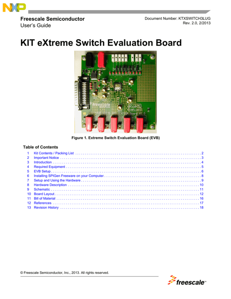
Figure 1. Extreme Switch Evaluation Board (EVB)
Table of Contents
1
2
3
4
5
6
7
8
9
10
11
12
13
Kit Contents / Packing List . . . . . . . . . . . . . . . . . . . . . . . . . . . . . . . . . . . . . . . . . . . . . . . . . . . . . . . . . . . . . . . . . . . 2
Important Notice . . . . . . . . . . . . . . . . . . . . . . . . . . . . . . . . . . . . . . . . . . . . . . . . . . . . . . . . . . . . . . . . . . . . . . . . . . . 3
Introduction . . . . . . . . . . . . . . . . . . . . . . . . . . . . . . . . . . . . . . . . . . . . . . . . . . . . . . . . . . . . . . . . . . . . . . . . . . . . . . . 4
Required Equipment . . . . . . . . . . . . . . . . . . . . . . . . . . . . . . . . . . . . . . . . . . . . . . . . . . . . . . . . . . . . . . . . . . . . . . . . 5
EVB Setup . . . . . . . . . . . . . . . . . . . . . . . . . . . . . . . . . . . . . . . . . . . . . . . . . . . . . . . . . . . . . . . . . . . . . . . . . . . . . . . . 6
Installing SPIGen Freeware on your Computer. . . . . . . . . . . . . . . . . . . . . . . . . . . . . . . . . . . . . . . . . . . . . . . . . . . . 8
Setup and Using the Hardware . . . . . . . . . . . . . . . . . . . . . . . . . . . . . . . . . . . . . . . . . . . . . . . . . . . . . . . . . . . . . . . . 9
Hardware Description . . . . . . . . . . . . . . . . . . . . . . . . . . . . . . . . . . . . . . . . . . . . . . . . . . . . . . . . . . . . . . . . . . . . . . 10
Schematic . . . . . . . . . . . . . . . . . . . . . . . . . . . . . . . . . . . . . . . . . . . . . . . . . . . . . . . . . . . . . . . . . . . . . . . . . . . . . . . 11
Board Layout . . . . . . . . . . . . . . . . . . . . . . . . . . . . . . . . . . . . . . . . . . . . . . . . . . . . . . . . . . . . . . . . . . . . . . . . . . . . . 12
Bill of Material . . . . . . . . . . . . . . . . . . . . . . . . . . . . . . . . . . . . . . . . . . . . . . . . . . . . . . . . . . . . . . . . . . . . . . . . . . . . 16
References . . . . . . . . . . . . . . . . . . . . . . . . . . . . . . . . . . . . . . . . . . . . . . . . . . . . . . . . . . . . . . . . . . . . . . . . . . . . . . 17
Revision History . . . . . . . . . . . . . . . . . . . . . . . . . . . . . . . . . . . . . . . . . . . . . . . . . . . . . . . . . . . . . . . . . . . . . . . . . . 18
© Freescale Semiconductor, Inc., 2013. All rights reserved.
Kit Contents / Packing List
1
Kit Contents / Packing List
•
•
Assembled and tested evaluation board/module in anti-static bag.
CD-ROM containing:
• Supporting documentation for featured device (including data sheet and user's guide)
• SPIGen software
• Warranty card
KTXSWITCH3LUG, Rev. 2.0
2
Freescale Semiconductor
Important Notice
2
Important Notice
Freescale provides the enclosed product(s) under the following conditions:
This evaluation kit is intended for use of ENGINEERING DEVELOPMENT OR EVALUATION
PURPOSES ONLY. It is provided as a sample IC pre-soldered to a printed circuit board to make it easier
to access inputs, outputs, and supply terminals. This EVB may be used with any development system or
other source of I/O signals by simply connecting it to the host MCU or computer board via off-the-shelf
cables. This EVB is not a Reference Design and is not intended to represent a final design
recommendation for any particular application. Final device in an application will be heavily dependent
on proper printed circuit board layout and heat sinking design as well as attention to supply filtering,
transient suppression, and I/O signal quality.
The goods provided may not be complete in terms of required design, marketing, and or manufacturing
related protective considerations, including product safety measures typically found in the end product
incorporating the goods. Due to the open construction of the product, it is the user's responsibility to take
any and all appropriate precautions with regard to electrostatic discharge. In order to minimize risks
associated with the customers applications, adequate design and operating safeguards must be provided
by the customer to minimize inherent or procedural hazards. For any safety concerns, contact Freescale
sales and technical support services.
Should this evaluation kit not meet the specifications indicated in the kit, it may be returned within 30 days
from the date of delivery and will be replaced by a new kit.
Freescale reserves the right to make changes without further notice to any products herein. Freescale
makes no warranty, representation or guarantee regarding the suitability of its products for any particular
purpose, nor does Freescale assume any liability arising out of the application or use of any product or
circuit, and specifically disclaims any and all liability, including without limitation consequential or
incidental damages. “Typical” parameters can and do vary in different applications and actual
performance may vary over time. All operating parameters, including “Typical”, must be validated for each
customer application by customer’s technical experts.
Freescale does not convey any license under its patent rights nor the rights of others. Freescale products
are not designed, intended, or authorized for use as components in systems intended for surgical implant
into the body, or other applications intended to support or sustain life, or for any other application in which
the failure of the Freescale product could create a situation where personal injury or death may occur.
Should Buyer purchase or use Freescale products for any such unintended or unauthorized application,
Buyer shall indemnify and hold Freescale and its officers, employees, subsidiaries, affiliates, and
distributors harmless against all claims, costs, damages, and expenses, and reasonable attorney fees
arising out of, directly or indirectly, any claim of personal injury or death associated with such unintended
or unauthorized use, even if such claim alleges that Freescale was negligent regarding the design or
manufacture of the part.Freescale™ and the Freescale logo are trademarks of Freescale Semiconductor,
Inc. All other product or service names are the property of their respective owners.
© Freescale Semiconductor, Inc. 2013
KTXSWITCH3LUG, Rev. 2.0
Freescale Semiconductor
3
Introduction
3
3.1
Introduction
EVB Features
This family of devices is designed for low-voltage automotive lighting applications. Its five low RDS(ON)
MOSFETs can control:
•
•
•
•
Five separate 55W / 28W bulbs
Five separate Xenon modules
Five separate LEDs
Five separate Other type of loads
In addition, this family of devices has the following features:
•
•
•
3.2
Programming, control, and diagnostics are accomplished using a 16-bit SPI interface.
Its output with selectable slew-rate allows to satisfy electromagnetic compatibility (EMC)
requirements.
Each output can be controlled with an internal PWM modulated clock signal.
Device Description/Features
The 10XS3535 or 35XS3500 is designed for low-voltage automotive and industrial lighting applications.
Its five low RDS(ON) MOSFETs can control the high sides of five separate resistive loads (bulbs,
Xenon-HID modules and LEDs).
Programming, control, and diagnostics are accomplished using a 16-bit SPI interface (3.3V or 5.0V).
Each output has its own PWM control via the SPI. The 10XS3535 and 35XS3500 have highly
sophisticated failure mode handling to provide high availability of the outputs. Its multi-phase control and
output edge shaping improves electromagnetic compatibility (EMC) behavior.
Features
•
•
•
•
•
•
•
•
•
•
•
•
Penta high side switches
16-bit SPI communication interface with daisy chain capability
Current sense output with SPI-programmable multiplex switch and Board Temperature Feedback
Digital diagnosis feature
PWM module with multi-phase feature including prescaler
LEDs control including accurate current sensing and low duty-cycle capability
Fully-protected switches
Over-current shutdown detection
Power net and reverse polarity protection
Low-power mode
Fail mode functions including auto restart feature
External smart power switch control including current recopy
KTXSWITCH3LUG, Rev. 2.0
4
Freescale Semiconductor
Required Equipment
3.3
KITUSBSPIEVME USB-to-Parallel Converter Board
The KITUSBSPIEVME board converts from USB to SPI and from USB to parallel data transmission. The
main function provided by this board is to allow a PC that may not have a parallel port to communicate
with other Freescale Evaluation Boards via a USB port.
.
Figure 2. KITUSBSPIEVME Converter Board
4
Required Equipment
Minimum required equipment:
• Power DC supply 40A/20V
• 5.0 V power supply, 1.0 A current capability
• Computer with an available USB port, running Windows XP or higher
• KITUSBSPIEVME board for converting from USB to SPI
• SPIGen software, which is available from the Freescale SPIGen website (also from the evaluation kit’s
CD-ROM)
• Typical load (lamps,...)
KTXSWITCH3LUG, Rev. 2.0
Freescale Semiconductor
5
EVB Setup
5
EVB Setup
The typical evaluation board (EVB) shown below utilizes the KITUSBSPIEVME as an alternate
communication interface to a PC, instead of a 25 pin parallel I/O connector/cable. These EVBs have been
designed to use SPIGen software in order to communicate and control the device functions on the
evaluation board. The figure below illustrates a typical EVB and how you would configure it to work with
a KITUSBSPIEVME interface board, for a USB connection to a PC.
Power
Supply
JC Connector
KITUSBSPIEVME
SPI
Communication
25-Pin Parallel
Connector
PCI via USB
Jumper Matrix
Extreme Switch
Evaluation Board
Figure 3. Evaluation Board Setup
Verify that the SI signal (Slave Input of the Serial Peripheral Input bus) on the EVB connects to the 25-pin
parallel connector on pin 3. If instead it is on pin 6, then the jumper matrix of the KITUSBSPIEVME
(Figure 4) will have to be configured in the following way:
1. Remove the jumper between pins SI and 3.
2. Remove the jumper between pins Data1 and 6.
3. Connect a jumper between pin SI and pin 6
KTXSWITCH3LUG, Rev. 2.0
6
Freescale Semiconductor
EVB Setup
Figure 4. Jumper Matrix on KITUSBSPIEVME Converter Board
KTXSWITCH3LUG, Rev. 2.0
Freescale Semiconductor
7
Installing SPIGen Freeware on your Computer
6
Installing SPIGen Freeware on your Computer
The latest version of SPIGen can be downloaded from the SPIGen web page at www.freescale.com (see
the References section) and is designed to run on any Windows 7, Vista or XP-based operating system.
SPIGen is also included on the CD-ROM supplied with the board, though this version may not be as
up-to-date as that available from the SPIGen web page.
Before you install the program, refer to the SPIGen README.txt file to check the compatibility of the
installation program and your computer operating system. For each operating system, README.txt
describes where the software should be installed.
For computers running Windows 7, Vista, or Windows XP, download the SPIGen 7 install program from
the SPIGen website. When the download is complete, run the install program. Several temporary files will
be copied to your computer, and then the Installation Wizard will guide you through the rest of the
process.
To install the software from the CD-ROM, insert the CD-ROM into your CD drive. Click the Start button,
and then click “Run…”.
To use SPIGen, go to the Windows Start menu, then Programs, then SPIGen, and click on the SPIGen
icon. The SPIGen Graphic User Interface (GUI) will appear. Go to the File menu in the upper left hand
corner of the GUI, and select Open. In the file selection window that appears, set the “Files of type: ”
drop-down menu to “All Files (*.*)”. Next, browse the evaluation kit CD-ROM and select the file called
“SPIGen Config File.txt”. Click Open, and SPIGen will create a specifically configured SPI command
generator for your EVB.
The GUI is shown in Figure 5. The text at the top is the name of the configuration file loaded. (As an
exceptional case, the file name has a .txt extension for the boards covered by this user’s guide. In other
cases, the standard .spi extension will be evident.) The left side panel displays folders that group user
interfaces. The boards associated with this guide will all make use of the Generic user interfaces. (The
other pre-installed folders contain interfaces for boards unrelated to this document.) The process of
loading the configuration files has assigned a list of “Extra Pins” as well as a list “Quick Commands”, all
of which are specific to the board in use.
KTXSWITCH3LUG, Rev. 2.0
8
Freescale Semiconductor
Setup and Using the Hardware
Figure 5. SPIGen GUI
7
Setup and Using the Hardware
Warning: Always wear Safety Glasses when working around electronic modules and when soldering.
1. The EVB allows the customer to quickly evaluate features of the device with a simple bench top setup. All switch
inputs may be evaluated using the onboard switch banks or actual system switches connected to the switch input
edge connector.
2. Using a standard 25 pin Sub-D parallel port cable to provide the Serial Peripheral Interface (SPI) communication
with this EVB (see SETUP_EVB).
3. Connect power supply to the VPWR and GND terminals on the EVB. Make sure the voltages provided are in
accordance with the device data sheet and that the supply currents are sufficient to supply the switch contact
wetting current
4. Connect desired external load between one of the output (OUT1 - OUT5) and power supply ground.
5. For direct control of the outputs apply +5V on connectors IGN, FLASH and FOG. Corresponding HS output
turns-on. Each IN input wakes the device.
KTXSWITCH3LUG, Rev. 2.0
Freescale Semiconductor
9
Hardware Description
8
8.1
Hardware Description
Jumper Connections
JMP1
Allows connecting current sensing resistor
1-2 selection: CSNS terminal connected to JP1 connector
2-3 selection: CSNS terminal connected through 1k Ohm resistor to ground
JMP2
Allows connecting ignition signal
1-2 selection: IGN terminal connected to JP2 connector
2-3 selection: 5V applied directly to IGN terminal
JMP3
Allows connecting flasher signal
1-2 selection: FLASHER terminal connected to JP3 connector
2-3 selection: 5V applied directly to FLASHER terminal
JMP4
Allows connecting limp home signal
1-2 selection: LIMP terminal connected to JP4 connector
2-3 selection: 5V applied directly to LIMP terminal
JMP5
Allows connecting PWM clock signal
1-2 selection: CLOCK terminal connected to JP7 connector
2-3 selection: CLOCK terminal connected to DB25 connector
JMP6
Allows connecting reset signal
1-2 selection: RSTB terminal connected to DB25 connector
2-3 selection: 5V applied directly to RSTB terminal
JMP7
Allows connecting fog signal
1-2 selection: FOG terminal connected to JP8 connector
2-3 selection: 5V applied directly to FOG terminal
JMP8
Allows disconnecting 5V reference voltage
JMP9 to JMP13
Allows disconnecting the LED on the corresponding output OUT1-5
TEST POINTS
Several test points are presented on the evaluation board to check some signals using oscilloscope if necessary.
KTXSWITCH3LUG, Rev. 2.0
10
Freescale Semiconductor
A
B
C
1
BANANA_RED
BANANA_RED
CN7
BANANA_RED
CN6
BANANA_RED
CN5
BANANA_RED
CN4
CN3
SOUT5
2
2
2
2
2
TP12
TSTPT
TSTPT
2PTS
2PTS
JMP10
2PTS
JMP9
2PTS
JMP13
2PTS
JMP12
JMP1
JUMP3
TSTPT
TP24
SOUT1
TSTPT
TP23
SOUT2
TSTPT
TP22
SOUT3
TSTPT
TP21
SOUT4
TP20
OUT5
OUT4
OUT3
OUT2
OUT1
1
JMP11
GND
47uF
BYD57 C2 +
C1
100nF
GND
BANANA_RED
CN2
VBAT D7
1
1
1
1
1
IN
JMP2
JUMP3
GND
OUT
U1
L7805CD2T
JP1
EM_2MM_BLANC
GND
R22
1k
1
2
3
CSNS
GND
2
GND
IGN
BANANA_BLACK
10k
R16
10k
R15
10k
R14
10k
R13
10k
R12
2
JP2
EM_2MM_BLANC
TSTPT
TP13
C3
1uF
GND
V_5V
3
JMP8
JMP3
JUMP3
GND
GND
GND
GND
GND
JP3
EM_2MM_BLANC
TSTPT
TP14
V_5V
D6 LEDV
D5 LEDV
D4 LEDV
D3 LEDV
D2 LEDV
GND
D1
LEDV
R1 2PTS
470
2
FLASH
D
JMP4
JUMP3
V_5V
1
LI MP
CN1
1
2
3
1
1
1
1
3
JP4
EM_2MM_BLANC
TSTPT
TP15
V_5V
3
GND
JMP7
JUMP3
J2
BNC
FOG
JP8
EM_2MM_BLANC
TSTPT
TP25
V_5V
VBAT
1nF
10nF
C6
C4
VBAT
J4
BNC
4
JP5
JP6
EM_2MM_BLANC
EM_2MM_BLANC
GND
OUT1
OUT2
OUT3
OUT4
OUT5
CSNS
CP
U3
C16
100nF
JMP5
JUMP3
22
21
20
19
18
CSNS 24
CP
16
C15
1uF
OUT5
SOUT5
OUT4
SOUT4
OUT3
SOUT3
OUT2
SOUT2
OUT1
SOUT1
TP4
TSTPT
C14
22uF
TP17
TSTPT
GND
TP16
TSTPT
10R
R2
100nF
C8
VBAT
TP19
TSTPT
GND
TP8 TP9 TP10 TP11
TSTPTTSTPTTSTPTTSTPT
4
TP18
TSTPT
15
VBAT
5
JP7
EM_2MM_BLANC
1
2
3
4
5
6
7
8
9
10
11
12
13
V_5V
MISO
FETOUT
FETIN
IGN
RSTB
FLASH
CLOCK
LIMP
FOG
CSB
SCLK
MOSI
GND
JMP6
JUMP3
R23
1k
V_5V
CORNERLIGHTPH4PQFN
FETIN
IGN
RESET
FLASHER
CLOCK
LIMP
FOG
CS
SCLK
SI
VCC
SO
FETOUT
SVBAT
5
GND
GND
GND
14
23
17
2
1
1
2
3
1
1
1
2
3
1
1
1
2
3
1
1
FETIN
1
1
FETOUT
1
1
1
2
3
CLOCK
CLK
1
1
2
3
Freescale Semiconductor
RSTB0
1k
R5
1k
R4
1k
R3
CLK
1k
6
R7
RSTB0 R6
1k
MOSI
SCLK
CSB
6
MISO
GND
GND
GND
GND
A3
OUT5
OUT4
OUT3
OUT2
OUT1
1nF
10nF
C26
C21
1nF
10nF
C25
C20
1nF
10nF
C24
C19
1nF
10nF
C23
C18
1nF
10nF
C22
C17
10
MC74HC4050
MC74HC4050
U2F
14
MC74HC4050
U2E
11
MC74HC4050
U2B
5
U2C
7
7
10R
R21
10R
R20
10R
R19
10R
R18
10R
R17
Number:1
7
Sheet1 of 1
Revision:1.4
PH4 Application Board
C13
22nF-dnp
C11
22nF-dnp
C9
22nF-dnp
C7
22nF-dnp
C5
22nF-dnp
Date: 14-Apr-2008
Size:
U2D
9
GND
MC74HC4050
3
U2A
MC74HC4050
GND
15
12
4
6
2
V_5V
Title Cornerlight
OUT5
OUT4
OUT3
OUT2
OUT1
TSTPT
TP7
TP6
TSTPT
TP5
TSTPT
TP3
TSTPT
TP2
TSTPT
TP1
TSTPT
1
8
8
GND
GND
GND
GND
GND
GND
1
14
2
15
3
16
4
17
5
18
6
19
7
20
8
21
9
22
10
23
11
24
12
25
13
J11
BNC
J9
BNC
J8
BNC
J7
BNC
J3
BNC
J1
DB25
8
A
B
C
D
9
RSTB
1
Schematic
Schematic
KTXSWITCH3LUG, Rev. 2.0
11
Board Layout
10 Board Layout
10.1
Assembly Layer Top
KTXSWITCH3LUG, Rev. 2.0
12
Freescale Semiconductor
Board Layout
10.2
Top Layer Routing
KTXSWITCH3LUG, Rev. 2.0
Freescale Semiconductor
13
Board Layout
10.3
Bottom Layer Routing
KTXSWITCH3LUG, Rev. 2.0
14
Freescale Semiconductor
Board Layout
10.4
Drill Location
KTXSWITCH3LUG, Rev. 2.0
Freescale Semiconductor
15
Bill of Material
11 Bill of Material
Part
Freescale
MC10XS3535PNA or MC35XS3500PNA
Footprint
PQFN24
Qty
Ref
1
U3
BANANA RED
6
CN2 CN3 CN4 CN5 CN6 CN7
BANANA BLACK
1
CN1
Capacitor 22uF 16V 10%
1812
1
C14
DB25
SUBD_25_MC
1
J1
NXP SCHOTTKY Diode PRLL5819 40V 1A
SOD87
1
D7
LED Green
LED1206
6
D1 D2 D3 D4 D5 D6
Capacitor C0805 100nF 50V 10%
C0805
2
C8 C16
Capacitor C1206 1uF 50V 10%
C1206
2
C3 C15
Capacitor 1812 47uF 10V 10%
1812
1
C2
Capacitor 1206 100nF 50V 10%
C1206
1
C1
Capacitor C1206 22nF DNP 50V 10%
C1206 DNP
5
C5 C7 C9 C11 C13
Capacitor C0805 1nF 50V 5%
C0805
6
C6 C22 C23 C24 C25 C26
Capacitor C0805 10nF 50V 10%
C0805
6
C4 C17 C18 C19 C20 C21
Test Point
5001
4
TP8 TP9 TP10 TP11
Test Point
5000
21
TP1 TP2 TP3 TP4 TP5 TP6 TP7 TP12 TP13 TP14 TP15
TP16 TP17 TP18 TP19 TP20 TP21 TP22 TP23 TP24 TP25
10k Resistor +/-1%
R1206
5
R12 R13 R14 R15 R16
NXP MC74HC4050
SO16
1
U2
STM l7805CD2T
D2PAK
1
U1
1k Resistor +/-1%
R1206
7
R3 R4 R5 R6 R7 R22 R23
Jumper
CON_2_2,54
6
JMP8 JMP9 JMP10 JMP11 JMP12 JMP13
Jumper
CON_3_2,54
7
JMP1 JMP2 JMP3 JMP4 JMP5 JMP6 JMP7
SMA Connector
SMA
7
J2 J3 J4 J7 J8 J9 J11 (Not Populated)
Resistor 10 +/-1%
R1206
6
R2 R17 R18 R19 R20 R21
Resistor 470 +/-1%
R1206
1
R1
KTXSWITCH3LUG, Rev. 2.0
16
Freescale Semiconductor
References
12 References
Following are URLs where you can obtain information on other Freescale products and application solutions:
Document
Number
MC10XS3535
MC35XS3500
Description
Data Sheet
Data Sheet
KITUSBSPIEVME
Tool Summary Page
SPIGen Reference
Tool Summary Page
Analog Home Page
Automotive Home Page
URL
www.freescale.com/files/analog/doc/data_sheet/MC10XS3535.pdf
www.freescale.com/files/analog/doc/data_sheet/MC35XS3500.pdf
http://www.freescale.com/webapp/sps/site/
prod_summary.jsp?code=KITUSBSPIEVME
http://www.freescale.com/files/soft_dev_tools/software/device_drivers/
SPIGen.html?fsrch=1&sr=11
www.freescale.com/analog
www.freescale.com/automotive
KTXSWITCH3LUG, Rev. 2.0
Freescale Semiconductor
17
Revision History
13 Revision History
Revision
1.0
2.0
Date
6/2010
2/2013
Description of Changes
Initial Release
• Provide information on the use of the KITUSBSPIEVME Converter Board for USB
connections.
• Updated Evaluation Board Setup diagram, SPIGen GUI image and PCB layer images.
KTXSWITCH3LUG, Rev. 2.0
18
Freescale Semiconductor
Revision History
KTXSWITCH3LUG, Rev. 2.0
Freescale Semiconductor
19
How to Reach Us:
Information in this document is provided solely to enable system and software
Home Page:
freescale.com
implementers to use Freescale products. There are no express or implied copyright
Web Support:
freescale.com/support
information in this document.
licenses granted hereunder to design or fabricate any integrated circuits on the
Freescale reserves the right to make changes without further notice to any products
herein. Freescale makes no warranty, representation, or guarantee regarding the
suitability of its products for any particular purpose, nor does Freescale assume any
liability arising out of the application or use of any product or circuit, and specifically
disclaims any and all liability, including without limitation consequential or incidental
damages. “Typical” parameters that may be provided in Freescale data sheets and/or
specifications can and do vary in different applications, and actual performance may
vary over time. All operating parameters, including “typicals,” must be validated for
each customer application by customer’s technical experts. Freescale does not convey
any license under its patent rights nor the rights of others. Freescale sells products
pursuant to standard terms and conditions of sale, which can be found at the following
address: http://www.reg.net/v2/webservices/Freescale/Docs/TermsandConditions.htm
Freescale, the Freescale logo, AltiVec, C-5, CodeTest, CodeWarrior, ColdFire, C-Ware,
Energy Efficient Solutions logo, mobileGT, PowerQUICC, QorIQ, Qorivva, StarCore, and
Symphony are trademarks of Freescale Semiconductor, Inc., Reg. U.S. Pat. & Tm. Off.
Airfast, BeeKit, BeeStack, ColdFire+, CoreNet, Flexis, MagniV, MXC, Platform in a
Package, Processor expert, QorIQ Qonverge, QUICC Engine, Ready Play,
SMARTMOS, TurboLink, Vybrid, and Xtrinsic are trademarks of Freescale
Semiconductor, Inc. All other product or service names are the property of their
respective owners.
© 2013 Freescale Semiconductor, Inc.
Document Number: KTXSWITCH3LUG
Rev. 2.0
2/2013
