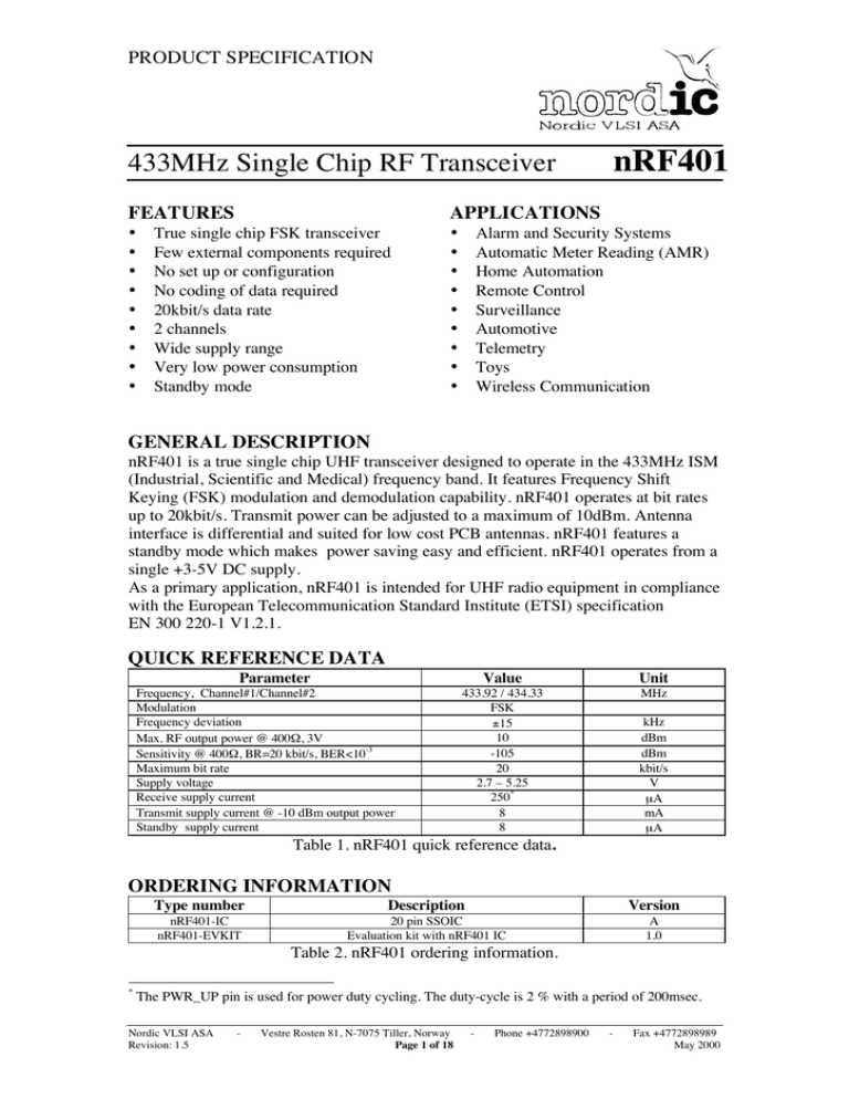
PRODUCT SPECIFICATION
nRF401
433MHz Single Chip RF Transceiver
FEATURES
APPLICATIONS
True single chip FSK transceiver
Few external components required
No set up or configuration
No coding of data required
20kbit/s data rate
2 channels
Wide supply range
Very low power consumption
Standby mode
•
•
•
•
•
•
•
•
•
Alarm and Security Systems
Automatic Meter Reading (AMR)
Home Automation
Remote Control
Surveillance
Automotive
Telemetry
Toys
Wireless Communication
•
•
•
•
•
•
•
•
•
GENERAL DESCRIPTION
nRF401 is a true single chip UHF transceiver designed to operate in the 433MHz ISM
(Industrial, Scientific and Medical) frequency band. It features Frequency Shift
Keying (FSK) modulation and demodulation capability. nRF401 operates at bit rates
up to 20kbit/s. Transmit power can be adjusted to a maximum of 10dBm. Antenna
interface is differential and suited for low cost PCB antennas. nRF401 features a
standby mode which makes power saving easy and efficient. nRF401 operates from a
single +3-5V DC supply.
As a primary application, nRF401 is intended for UHF radio equipment in compliance
with the European Telecommunication Standard Institute (ETSI) specification
EN 300 220-1 V1.2.1.
QUICK REFERENCE DATA
Parameter
Frequency, Channel#1/Channel#2
Modulation
Frequency deviation
Max. RF output power @ 400Ω, 3V
Sensitivity @ 400Ω, BR=20 kbit/s, BER<10-3
Maximum bit rate
Supply voltage
Receive supply current
Transmit supply current @ -10 dBm output power
Standby supply current
Value
Unit
433.92 / 434.33
FSK
±15
10
-105
20
2.7 – 5.25
250*
8
8
MHz
kHz
dBm
dBm
kbit/s
V
µA
mA
µA
Table 1. nRF401 quick reference data.
ORDERING INFORMATION
Type number
Description
Version
nRF401-IC
nRF401-EVKIT
20 pin SSOIC
Evaluation kit with nRF401 IC
A
1.0
Table 2. nRF401 ordering information.
*
The PWR_UP pin is used for power duty cycling. The duty-cycle is 2 % with a period of 200msec.
Nordic VLSI ASA
Revision: 1.5
-
Vestre Rosten 81, N-7075 Tiller, Norway
Page 1 of 18
-
Phone +4772898900
-
Fax +4772898989
May 2000
PRODUCT SPECIFICATION
nRF401 Single Chip RF Transceiver
BLOCK DIAGRAM
DOUT
TXEN
CS
DIN
PWR_UP
DEM
10
LNA
19
16
12
9
15
OSC
18
PLL
20
1
VCO
4
5
ANT1
ANT2
PA
6
11
RF_PWR
VCO
INDUCTOR
LOOP
FILTER
REFERENCE
Figure 1. nRF401 block diagram with external components.
PIN FUNCTIONS
Pin
Name
Pin function
Description
1
2
3
4
5
6
7
8
9
10
11
12
XC1
VDD
VSS
FILT1
VCO1
VCO2
VSS
VDD
DIN
DOUT
RF_PWR
CS
Input
Power
Ground
Input
Input
Input
Ground
Power
Input
Output
Input
Input
13
14
15
16
17
18
VDD
VSS
ANT2
ANT1
VSS
PWR_UP
Power
Ground
Input/Output
Input/Output
Ground
Input
19
TXEN
Input
20
XC2
Output
Crystal oscillator input
Power supply (+3-5V DC)
Ground (0V)
Loop filter
External inductor for VCO
External inductor for VCO
Ground (0V)
Power supply (+3-5V DC)
Data input
Data output
Transmit power setting
Channel selection
CS=“0” ⇒ 433.92MHz (Channel#1)
CS=“1” ⇒ 434.33MHz (Channel#2)
Power supply (+3-5V DC)
Ground (0V)
Antenna terminal
Antenna terminal
Ground (0V)
Power on/off
PWR_UP = “1” ⇒ Power up (Operating mode)
PWR_UP = “0” ⇒ Power down (Standby mode)
Transmit enable
TXEN = “1” ⇒ Transmit mode
TXEN = “0” ⇒ Receive mode
Crystal oscillator output
Table 3. nRF401 pin functions.
Nordic VLSI ASA Revision: 1.5
Vestre Rosten 81, N-7075 Tiller, Norway Page 2 of 18
Phone +4772898900
-
Fax +4772898989
May 2000
PRODUCT SPECIFICATION
nRF401 Single Chip RF Transceiver
ELECTRICAL SPECIFICATIONS
Conditions: VDD = +3V DC, VSS = 0V, TA= -25°C to +85°C
Symbol
VDD
VSS
IDD
PRF
VIH
VIL
VOH
VOL
IH
IL
f1
f2
Δf
fIF
BWIF
fXTAL
ZI
Parameter (condition)
Min.
Typ.
Max.
Units
Supply voltage
2.7
3
5.25
V
Ground
0
V
Total current consumption
Receive mode
11
mA
Transmit mode @ -10 dBm RF power
8
mA
Stand by mode
8
µA
10
dBm
Max. RF output power @ 400Ω load
Logic “1” input voltage
VDD
V
0.7⋅VDD
Logic “0” input voltage
0
V
0.3⋅VDD
Logic “1” output voltage (IOH = - 1.0mA)
VDD
V
0.7⋅VDD
Logic “0” output voltage (IOL = 1.0mA)
0
V
0.3⋅VDD
Logic “1” input current (VI = VDD)
+20
µA
Logic “0” input current (VI = VSS)
-20
µA
Channel#1 frequency
433.92
MHz
Channel#2 frequency
434.33
MHz
Dynamic range
90
dB
Modulation type
FSK
Frequency deviation
kHz
±15
IF frequency
400
kHz
IF bandwidth
65
85
kHz
Crystal frequency
4.0
MHz
Crystal frequency stability requirement 1)
ppm
±45
-105
dBm
Sensitivity @ 400Ω,BR=20 kbit/s, BER < 10-3
Bit rate
0
20
kbit/s
Recommended antenna port differential impedance
400
Ω
Spurious emission
Compliant with EN 300-220-1 V1.2.1 2)
Table 4. nRF401 electrical specifications.
1)
2)
Maximum 5dB sensitivity degradation at temperature extremes. See also page 11.
With a PCB loop antenna or a differential to single ended matching network to a 50Ω antenna.
ABSOLUTE MAXIMUM RATINGS
Supply voltages
VDD .............................. - 0.3V to +6V
VSS ................................................ 0V
Input voltage
VI ...................... - 0.3V to VDD + 0.3V
Output voltage
VO ..................... - 0.3V to VDD + 0.3V
Power dissipation
PD (TA=25°C)........................... 250mW
Temperatures
Operating Temperature…. -25°C to +85°C
Storage Temperature…... -40°C to +125°C
Note: Stress exceeding one or more of the limiting values may cause permanent
damage to the device.
ATTENTION!
Electrostatic Sensitive Device
Observe Precaution for handling
Nordic VLSI ASA Revision: 1.5
Vestre Rosten 81, N-7075 Tiller, Norway Page 3 of 18
Phone +4772898900
-
Fax +4772898989
May 2000
PRODUCT SPECIFICATION
nRF401 Single Chip RF Transceiver
PIN ASSIGNMENT
XC1
1
VDD
2
20 XC2
19 TXEN
VSS
3
nRF401
FILT1
4
20 pin SSOIC
VCO1
5
16 ANT1
VCO2
6
15 ANT2
VSS
7
14 VSS
VDD
8
13 VDD
DIN
9
12 CS
DOUT
10
11 RF_PWR
18 PWR_UP
17 VSS
Figure 2. nRF401 pin assignment.
PACKAGE OUTLINE
nRF401, 20 pin SSOIC. (Dimensions in mm.)
20 19 18
E
H
1 2 3
D
A1 A
e
Package Type
20 pin SSOIC
(Wide)
b
Min
Max
α
L
D
6.90
7.50
E
5.00
5.60
H
7.40
8.20
A
2.00
A1
0.05
e
0.65
b
0.22
0.38
L
0.55
0.95
Copl.
0.10
α
0°
8°
Figure 3. SSOIC-20 Package outline.
Nordic VLSI ASA Revision: 1.5
Vestre Rosten 81, N-7075 Tiller, Norway Page 4 of 18
Phone +4772898900
-
Fax +4772898989
May 2000
PRODUCT SPECIFICATION
nRF401 Single Chip RF Transceiver
IMPORTANT TIMING DATA
Timing information
The timing information for the different operations is summarised in Table 5.
(TX is transmit mode, RX is receive mode and Std.by is Standby mode.)
Change of Mode
TX RX
RX TX
Std.by TX
Std.by RX
VDD=0 TX
VDD =0 RX
Name
tTR
tRT
tST
tSR
tVT
tVR
Max Delay
3ms
1ms
2ms
3ms
4ms
5ms
Condition
Operational
mode
Start-up
Table 5 Switching times for nRF401.
Switching TX ↔ RX (operational mode).
When switching from RX-mode to TX-mode data (DIN) may not be sent before the
TXEN-input has been high for at least 1ms, see Figure 4(a).
When switching from TX-mode to RX-mode the receiver may not receive data
(DOUT) before the TXEN-input has been low for at least 3ms, see Figure 4(b).
RX to TX
TX to RX
VDD
VDD
PWR_UP
PWR_UP
TXEN
TXEN
DIN
DOUT
1ms
3ms
ms
0
2
4
(a)
ms
0
2
4
(b)
Figure 4. Timing diagram for nRF401for switching from RX to TX (a)
and TX to RX (b).
Switching between standby and RX-mode (operational mode).
The time from the PWR_UP input is set to “1”, until the data (DOUT) is valid is tSR,,
see Table 5. Worst case tSR is 3ms for nRF401 as can be seen in Figure 5 (a).
Switching between standby and TX-mode (operational mode).
The time from the PWR_UP input is set to “1”, until the synthesised frequency is
stable is tST, see Table 5.
Nordic VLSI ASA Revision: 1.5
Vestre Rosten 81, N-7075 Tiller, Norway Page 5 of 18
Phone +4772898900
-
Fax +4772898989
May 2000
PRODUCT SPECIFICATION
nRF401 Single Chip RF Transceiver
Std.by to RX
Std.by to TX
VDD
VDD
PWR_UP
PWR_UP
TXEN
TXEN
DOUT
DIN
3ms
1ms1ms
ms
0
2
ms
4
0
2
4
(b)
(a)
Figure 5 Timing diagram for nRF401 when going from standby to RX-mode (a) or
TX-mode (b).
Power up to transmit-mode (start-up).
To avoid spurious emission outside the ISM-band when the power supply is switched
on, the TXEN-input must be kept low until the synthesised frequency is stable, see
Figure 6 (a).
When enabling transmit-mode, TXEN-input should be high for at least 1 ms before
data (DIN) is transmitted, see Figure 6 (a).
VDD=0 to TX
VDD=0 to RX
VDD
VDD
PWR_UP
PWR_UP
TXEN
TXEN
DIN
DOUT
3ms
1ms
2
4
5ms
ms
0
(a)
ms
0
2
4
6
(b)
Figure 6. Timing diagram for nRF401 when powering up to TX-mode (a)
or RX-mode (b).
Power up to receive mode (start up).
In transition from power up to receive mode, the receiver may not receive data
(DOUT) until VDD has been stable (VDD > 2.7 V) for at least 5ms, see Figure 6(b).
If an external reference oscillator is used, the receiver may receive data (DOUT) after
3ms.
Nordic VLSI ASA Revision: 1.5
Vestre Rosten 81, N-7075 Tiller, Norway Page 6 of 18
Phone +4772898900
-
Fax +4772898989
May 2000
PRODUCT SPECIFICATION
nRF401 Single Chip RF Transceiver
APPLICATION INFORMATION
Antenna input/output
The ANT1 and ANT2 pins provide RF input to the LNA (Low Noise Amplifier) when
nRF401 is in receive mode, and RF output from the PA (Power Amplifier) when
nRF401 is in transmit mode. The antenna connection to nRF401 is differential and the
recommended load impedance at the antenna port is 400Ω.
Figure 12 shows a typical application schematic with a differential loop antenna on a
Printed Circuit Board (PCB). The output stage (PA) consists of two open collector
transistors in a differential pair configuration. VDD to the PA must be supplied
through the collector load. When connecting a differential loop antenna to the
ANT1/ANT2 pins, VDD should be supplied through the centre of the loop antenna as
shown in Figure 12.
A single ended antenna or 50Ω test instrument may be connected to nRF401 by using
a differential to single ended matching network (BALUN) as shown in Figure 7.
180nH
RF in/out 50 ohm
18nH
ANT1
470pF
nRF401
1.8pF
VDD
ANT2
18nH
Figure 7. Connection of nRF401 to single ended antenna by using
a differential to single ended matching network.
The 180nH inductor to VDD in Figure 7, need to have a Self-Resonance Frequency
(SRF) above 433 MHz to be effective. Suitable inductors are listed in Table 6.
Vendors
WWW address
Stetco
Coilcraft
muRata
http://www.stetco.com
http://www.coilcraft.com
http://www.murata.com
Part. no., 180 nH inductors,
0603 size
0603G181KTE
0603CS-R18XJBC
LQW1608AR18J00
Table 6. Vendors and part. no. for suitable 180nH inductors.
Nordic VLSI ASA Revision: 1.5
Vestre Rosten 81, N-7075 Tiller, Norway Page 7 of 18
Phone +4772898900
-
Fax +4772898989
May 2000
PRODUCT SPECIFICATION
nRF401 Single Chip RF Transceiver
An additional notch filter (L and C) at the 50Ω RF input/output may be necessary
dependent on the application requirements (see application note nAN400-05).
A single ended antenna may also be connected to nRF401 using an 8:1 impedance RF
transformer. The RF transformer must have a centre tap at the primary side for VDD
supply.
RF output power
The external bias resistor R3 connected between the RF_PWR pin and VSS sets the
output power. The RF output power may be set to levels up to +10dBm. In Figure 8
the output power is plotted for power levels down to, but not limited to, -8.5dBm for a
differential load of 400Ω. DC power supply current versus external bias resistor value
is shown in Figure 9.
RF Output Power
10
22
8
27
33
6
39
4
47
2
56
0
68
82
-2
100
-4
120
-6
150
-8
180
-10
0
20
40
60
80
100
120
140
160
180
200
Ω]
Resistor Value [kΩ
Figure 8. RF output power vs. external power setting resistor (R3) for nRF401.
Total Chip Current
30,0
22
Current Consumption [mA]
25,0
27
20,0
33
39
47
15,0
56
68
82
10,0
100
120
150
180
5,0
0,0
0
20
40
60
80
100
120
140
160
180
200
Resistor Value [kΩ
Ω]
Figure 9. Total chip current consumption vs. external power setting resistor (R3) for
nRF401.
Nordic VLSI ASA Revision: 1.5
Vestre Rosten 81, N-7075 Tiller, Norway Page 8 of 18
Phone +4772898900
-
Fax +4772898989
May 2000
PRODUCT SPECIFICATION
nRF401 Single Chip RF Transceiver
PLL loop filter
The synthesiser loop filter is an external, single-ended second order lag-lead filter.
The recommended filter component values are: C3 = 820 pF, C4 =15 nF, and
R2 = 4.7 kΩ, see Figure 12.
VCO inductor
An external 22nH inductor connected between the VCO1 and VCO2 pins is required
for the on-chip voltage controlled oscillator (VCO). This inductor should be a high
quality chip inductor, Q > 45 @ 433 MHz, with a maximum tolerance of ± 2%. The
following 22 nH inductors (0603) are suitable for use with nRF401.
Vendors
WWW address
Pulse
Coilcraft
muRata
Stetco
KOA
http://www.pulseeng.com
http://www.coilcraft.com
http://www.murata.com
http://www.stetco.com
http://www.koaspeer.com
Part. no., 22 nH inductors, 0603
size
PE-0603CD220GTT
0603CS-22NXGBC
LQW1608A22NG00
0603G220GTE
KQ0603TE22NG
Table 7. Vendors and part no. for suitable 22nH inductors.
See page 11 and 12 for PCB layout guidelines regarding placement of the inductor.
Crystal specification
To achieve an active crystal oscillator (XOSC) with low power consumption, certain
requirements apply for crystal loss and capacitive load.
The crystal specification is:
f= 4.0000 MHz
Co ≤ 5 pF
ESR ≤150 ohm .
C L ≤ 14 pF
Crystal parallel resonant frequency
Crystal parallel equivalent capacitance
Crystal equivalent series resistance
Total crystal load capacitance, including capacitance in PCB
layout.
For the crystal oscillator shown in Figure 10 the load capacitance becomes:
CL =
C1´⋅ C 2´
,
C1´ + C 2 ´ Where C1´ = C1 + CPCB1 and C2´ = C2 + CPCB2
C1 and C2 are 0603 SMD capacitors as shown in the application schematic, see
Figure 12 and Table 9. CPCB1 and CPCB2 are the layout parasitic capacitance on the
circuit board.
Nordic VLSI ASA Revision: 1.5
Vestre Rosten 81, N-7075 Tiller, Norway Page 9 of 18
Phone +4772898900
-
Fax +4772898989
May 2000
PRODUCT SPECIFICATION
nRF401 Single Chip RF Transceiver
Crystal
oscillator
Crystal
equivalent
Co
Internal
R
External
components
Cs
ESR
L
Crystal
C1
C2
Figure 10. Crystal oscillator and crystal equivalent.
Sharing a reference crystal with a micro-controller
Figure 11 shows circuit diagram of a typical application where nRF401 and a micro
controller share the reference crystal.
micro
controller
X1
1.0M
R
XC1
nRF401
C
X2
XC2
5.6pF
C1
22pF
4.0 MHz
C2
22pF
Figure 11. nRF401 and a micro-controller sharing the reference crystal.
The crystal reference line from the micro-controller should not be routed close to full
swing digital data or control signals.
Transmit/receive mode selection
TXEN is a digital input for selection of transmit or receive mode.
TXEN = “1” selects transmit mode.
TXEN = “0” selects receive mode.
Channel#1 / Channel#2 selection
CS is a digital input for selection of either channel#1 (f1=433.92MHz)
or channel#2 (f2=434.33MHz).
CS = “0” selects channel#1.
CS = “1” selects channel#2.
Nordic VLSI ASA Revision: 1.5
Vestre Rosten 81, N-7075 Tiller, Norway Page 10 of 18
Phone +4772898900
-
Fax +4772898989
May 2000
PRODUCT SPECIFICATION
nRF401 Single Chip RF Transceiver
TXEN
0
0
1
1
X
Input
CS
0
1
0
1
X
PWR_UP
1
1
1
1
0
Response
Channel #
Mode
1
RX
2
RX
1
TX
2
TX
-Standby
Table 8. Required setting for standby and channel selection in RX and TX.
DIN (data input) and DOUT (data output)
The DIN pin is the input to the digital modulator of the transmitter. The input signal
to this pin should be standard CMOS logic level at data rates up to 20 kbit/s. No
coding of data is required.
DIN = “1” → f = f0 + Δf
DIN = “0” → f = f0 - Δf
The demodulated digital output data appear at the DOUT pin at standard CMOS logic
levels.
f0 + Δf → DOUT=“1”,
f0 - Δf → DOUT=“0”.
Power up
PWR_UP is a digital input for selection of normal operating mode or standby mode.
PWR_UP = “1” selects normal operating mode.
PWR_UP = “0” selects standby mode.
Frequency difference between transmitter and receiver
For optimum performance, the total frequency difference between transmitter and
receiver should not exceed 70 ppm (30 kHz). This yields a crystal stability
requirement of ±35 ppm for the transmitter and receiver. Frequency difference
exceeding this will result in a -12dB/octave drop in receiver sensitivity. The
functional frequency window of the transmission link is typically 450 ppm (200 kHz).
Example: A crystal with ±20 ppm frequency tolerance and ±25 ppm frequency
stability over the operating temperature has a worst case frequency difference of ±45
ppm. If the transmitter and receiver operate in different temperature environments, the
resulting worst-case frequency difference may be as high as 90 ppm. Resulting drop
in sensitivity due to the extra 20 ppm, is then approx. 5dB.
PCB layout and decoupling guidelines
A well-designed PCB is necessary to achieve good RF performance. A PCB with a
minimum of two layers including a ground plane is recommended for optimum
performance.
The nRF401 DC supply voltage should be decoupled as close as possible to the VDD
pins with high performance RF capacitors, see Table 9. It is preferable to mount a
Nordic VLSI ASA Revision: 1.5
Vestre Rosten 81, N-7075 Tiller, Norway Page 11 of 18
Phone +4772898900
-
Fax +4772898989
May 2000
PRODUCT SPECIFICATION
nRF401 Single Chip RF Transceiver
large surface mount capacitor (e.g. 2.2 µF ceramic) in parallel with the smaller value
capacitors. The nRF401 supply voltage should be filtered and routed separately from
the supply voltages of any digital circuitry.
Long power supply lines on the PCB should be avoided. All device grounds, VDD
connections and VDD bypass capacitors must be connected as close as possible to the
nRF401 IC. For a PCB with a topside RF ground plane, the VSS pins should be
connected directly to the ground plane. For a PCB with a bottom ground plane, the
best technique is to have via holes in or close to the VSS pads.
Full swing digital data or control signals should not be routed close to the PLL loop
filter components or the external VCO inductor.
The VCO inductor placement is important. The optimum placement of the VCO
inductor gives a PLL loop filter voltage of 1.1 ±0.2 V, which can be measured at
FILT1 (pin4). For a 0603 size inductor the length between the centre of the
VCO1/VCO2 pad and the centre of the inductor pad should be 5.4 mm, see Figure 13
(c) (layout, top view), for a 2 layer, 1.6 mm thick FR4 PCB.
PCB layout example
Figure 13 shows a PCB layout example for the application schematic in Figure 12.
A double-sided FR-4 board of 1.6mm thickness is used. This PCB has a continuous
ground plane on the bottom layer. Additionally, there are ground areas on the
component side of the board to ensure sufficient grounding of critical components. A
large number of via holes connect the top layer ground areas to the bottom layer
ground plane. There is no ground plane beneath the antenna.
For more layout information, please refer to application note nAN400-05,
“nRF401 RF and antenna layout.
Nordic VLSI ASA Revision: 1.5
Vestre Rosten 81, N-7075 Tiller, Norway Page 12 of 18
Phone +4772898900
-
Fax +4772898989
May 2000
PRODUCT SPECIFICATION
nRF401 Single Chip RF Transceiver
APPLICATION SCHEMATIC
+3V
R1
1M
0603
C5
2.2uF
1206
X1
4.000 MHz
C1
22pF
0603
C2
22pF
0603
REFERENCE
U1
C4
15nF
0603
C3
820pF
0603
L1
22nH
0603
R2
4.7K
0603
C6
100nF
0603
C7
1nF
0603
DIN
DOUT
1
2
3
4
5
6
7
8
9
10
XC1
VDD
VSS
FILT1
VCO1
VCO2
VSS
VDD
DIN
DOUT
XC2
TXEN
PWR_UP
VSS
ANT1
ANT2
VSS
VDD
CS
RF_PWR
nRF401
433MHz Single Chip RF Transceiver
SSOIC20
20
19
18
17
16
15
14
13
12
11
TXEN
PWR_UP
C10
3.3pF
0603
C9
100pF
0603
CS
R3
22K
0603
C8
100pF
0603
PLL FILTER
C11
5.6pF
0603
R4
18K aaaaaaaa
0603
J1
Loop antenna
25x15mm
Q=55
Figure 12. nRF401 application schematic.
Component
C1
C2
C3
C4
C5
C6
C7
C8
C9
C10
C11
L1
R1
R2
R3
R4
X1
Description
NP0 ceramic chip capacitor, (Crystal oscillator)
NP0 ceramic chip capacitor, (Crystal oscillator)
X7R ceramic chip capacitor, (PLL loop filter)
X7R ceramic chip capacitor, (PLL loop filter)
X7R ceramic chip capacitor, (Supply decoupling)
X7R ceramic chip capacitor, (Supply decoupling)
X7R ceramic chip capacitor, (Supply decoupling)
NP0 ceramic chip capacitor, (Supply decoupling)
NP0 ceramic chip capacitor, (Supply decoupling)
NP0 ceramic chip capacitor, (Antenna tuning)
NP0 ceramic chip capacitor, (Antenna tuning)
VCO inductor, Q>45 @ 433 MHz
0.1W chip resistor, (Crystal oscillator)
0.1W chip resistor, (PLL loop filter)
0.1W chip resistor, (Transmitter power setting)
0.1W chip resistor, (Antenna Q reduction)
Crystal
Size
Value
0603
0603
0603
0603
1206
0603
0603
0603
0603
0603
0603
0603
0603
0603
0603
0603
-
22
22
820
15
2.2
100
1
100
100
3.3
5.6
22
1.0
4.7
22
18
4.000
Tolerance
±0.1
±0.25
±2%
Table 9. Recommended External Components.
Nordic VLSI ASA Revision: 1.5
Vestre Rosten 81, N-7075 Tiller, Norway Page 13 of 18
Phone +4772898900
-
Fax +4772898989
May 2000
Units
pF
pF
pF
nF
µF
nF
nF
pF
pF
pF
pF
nH
MΩ
kΩ
kΩ
kΩ
MHz
PRODUCT SPECIFICATION
nRF401 Single Chip RF Transceiver
a) Top silk screen
b) Bottom silk screen
c) Top view
d) Bottom view
Figure 13. PCB layout (example) for nRF401 with loop antenna.
Nordic VLSI ASA Revision: 1.5
Vestre Rosten 81, N-7075 Tiller, Norway Page 14 of 18
Phone +4772898900
-
Fax +4772898989
May 2000
PRODUCT SPECIFICATION
nRF401 Single Chip RF Transceiver
DEFINITIONS
Data sheet status
Objective product specification
Preliminary product
specification
Product specification
This datasheet contains target specifications for product development.
This datasheet contains preliminary data; supplementary data may be
published from Nordic VLSI ASA later.
This datasheet contains final product specifications. Nordic VLSI ASA
reserves the right to make changes at any time without notice in order to
improve design and supply the best possible product.
Limiting values
Stress above one or more of the limiting values may cause permanent damage to the device. These are stress
ratings only and operation of the device at these or at any other conditions above those given in the
Specifications sections of the specification is not implied. Exposure to limiting values for extended periods may
affect device reliability.
Application information
Where application information is given, it is advisory and does not form part of the specification.
Table 10. Definitions.
Nordic VLSI ASA reserves the right to make changes without further notice to the
product to improve reliability, function or design. Nordic VLSI does not assume any
liability arising out of the application or use of any product or circuits described
herein.
LIFE SUPPORT APPLICATIONS
These products are not designed for use in life support appliances, devices, or systems
where malfunction of these products can reasonably be expected to result in personal
injury. Nordic VLSI ASA customers using or selling these products for use in such
applications do so at their own risk and agree to fully indemnify Nordic VLSI ASA
for any damages resulting from such improper use or sale.
Product specification: Revision Date: 26.05.2000.
Datasheet order code: 260500nRF401
All rights reserved ®. Reproduction in whole or in part is prohibited without the prior
written permission of the copyright holder.
Nordic VLSI ASA Revision: 1.5
Vestre Rosten 81, N-7075 Tiller, Norway Page 15 of 18
Phone +4772898900
-
Fax +4772898989
May 2000
PRODUCT SPECIFICATION
nRF401 Single Chip RF Transceiver
YOUR NOTES
Nordic VLSI ASA Revision: 1.5
Vestre Rosten 81, N-7075 Tiller, Norway Page 16 of 18
Phone +4772898900
-
Fax +4772898989
May 2000
PRODUCT SPECIFICATION
nRF401 Single Chip RF Transceiver
YOUR NOTES
Nordic VLSI ASA Revision: 1.5
Vestre Rosten 81, N-7075 Tiller, Norway Page 17 of 18
Phone +4772898900
-
Fax +4772898989
May 2000
PRODUCT SPECIFICATION
nRF401 Single Chip RF Transceiver
Nordic VLSI - World Wide Distributors
For Your nearest dealer, please see http://www.nvlsi.no
Main Office:
Vestre Rosten 81, N-7075 Tiller, Norway
Phone: +47 72 89 89 00, Fax: +47 72 89 89 89
E-mail: nRF@nvlsi.no
Visit the Nordic VLSI ASA website at http://www.nvlsi.no
Revision: 1.5
Page 18 of 18
May 2000
