DuettoDC CXA3345GL
advertisement

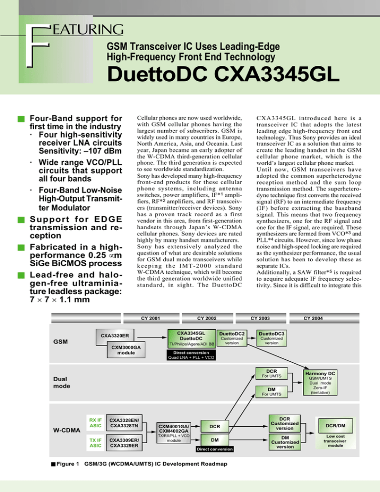
GSM Transceiver IC Uses Leading-Edge High-Frequency Front End Technology DuettoDC CXA3345GL ■ Four-Band support for first time in the industry · Four high-sensitivity receiver LNA circuits Sensitivity: –107 dBm · Wide range VCO/PLL circuits that support all four bands · Four-Band Low-Noise High-Output Transmitter Modulator ■ Support for EDGE transmission and reception ■ Fabricated in a highperformance 0.25 µm SiGe BiCMOS process ■ Lead-free and halogen-free ultraminiature leadless package: 7 × 7 × 1.1 mm Cellular phones are now used worldwide, with GSM cellular phones having the largest number of subscribers. GSM is widely used in many countries in Europe, North America, Asia, and Oceania. Last year, Japan became an early adopter of the W-CDMA third-generation cellular phone. The third generation is expected to see worldwide standardization. Sony has developed many high-frequency front-end products for these cellular phone systems, including antenna switches, power amplifiers, IF*1 amplifiers, RF*2 amplifiers, and RF transceivers (transmitter/receiver devices). Sony has a proven track record as a first vendor in this area, from first-generation handsets through Japan’s W-CDMA cellular phones. Sony devices are rated highly by many handset manufacturers. Sony has extensively analyzed the question of what are desirable solutions for GSM dual mode transceivers while keeping the IMT-2000 standard W-CDMA technique, which will become the third generation worldwide unified standard, in sight. The DuettoDC CY 2001 CXA3320ER GSM CXM3000GA module CY 2002 CXA3345GL DuettoDC CXA3345GL introduced here is a transceiver IC that adopts the latest leading edge high-frequency front end technology. Thus Sony provides an ideal transceiver IC as a solution that aims to create the leading handset in the GSM cellular phone market, which is the world’s largest cellular phone market. Until now, GSM transceivers have adopted the common superheterodyne reception method and the sum loop transmission method. The superheterodyne technique first converts the received signal (RF) to an intermediate frequency (IF) before extracting the baseband signal. This means that two frequency synthesizers, one for the RF signal and one for the IF signal, are required. These synthesizers are formed from VCO*3 and PLL*4 circuits. However, since low phase noise and high-speed locking are required as the synthesizer performance, the usual solution has been to develop these as separate ICs. Additionally, a SAW filter*5 is required to acquire adequate IF frequency selectivity. Since it is difficult to integrate this CY 2003 CY 2004 DuettoDC2 DuettoDC3 Customized version Customized version TI/Philips/Agere/ADI BB Direct conversion Quad LNA + PLL + VCO DCR For UMTS Dual mode DM For UMTS RX IF ASIC CXA3328EN/ CXA3328TN TX IF ASIC CXA3309ER/ CXA3329ER W-CDMA CXM4001GA/ CXM4002GA TX/RX/PLL + VCO module DCR DM Direct conversion ■ Figure 1 GSM/3G (WCDMA/UMTS) IC Development Roadmap DCR Customized version DM Customized version Harmony DC GSM/UMTS Dual mode Zero-IF (tentative) DCR/DM Low cost transceiver module component on an IC chip, an external component is used. Another issue is that although the sum loop technique used for transmission is effective at reducing transmission noise, it requires a power VCO circuit in the output block for transmission. To overcome these problems, Sony has developed, for the CXA3345GL, both a direct conversion receiver for the receiver block and a direct modulation transmitter for the transmitter block. These new approaches allowed Sony to create an ideal GSM transceiver solution. The GSM system for cellular phones is the system used in the most regions worldwide. As long as you have a handset*6 that supports the frequency bands allocated for the countries you will be traveling to, travelers and businessmen who go from country to country will be able to use the same GSM cellular phone they use in their home country in the same way, i.e. with the same phone number. Up to now, the main services have been the 900 MHz band and 1800 MHz band services used in Europe, Asia, and Oceania, and the 1900 MHz band in North America. The 850 MHz band service used in the US has been added to this list. By supporting all 4 of these bands, the CXA3345GL supports all GSM cellular phone frequency bands used worldwide. IF: Intermediate frequency RF: Radio frequency VCO: Voltage controlled oscillator PLL: Phase locked loop SAW filter: Surface acoustic wave filter New product: CXA3345GL Conventional product:CXM3000GA Package: LFLGA-60P-01 IF SAW LNA 1800 RF SAW LNA 900 RF SAW LNA 850 RF SAW LNA Loop filter I Q CXA3345GL VCO PLL Div 1800/1900 Sum RF SAW APC RF SAW 900 I Sum 850 RF SAW LNA RF SAW LNA I RF SAW Q Div LNA monitor Div I Loop filter RF SAW RF SAW Q CXM3000G Sum Control ■ Figure 2 CXA3345GL Block Diagram Q RF VCO PLL1 IF VCO PLL2 Base band 1900 RF SAW Base band Easy SW Package: VFLGA-84P-01 SW *1 *2 *3 *4 *5 *6: There are several handsets, including dual band (the 900 MHz/1800 MHz handset), triple band (the 900 MHz/1800 MHz/1900 MHz handset), and quad band (the 850 MHz/ 900 MHz/1800 MHz/1900 MHz handset), and there are handsets that fit particular uses, such as Europe-only handsets, or dual Europe/USA handsets. Four-Band Support for First Time in the Industry this device must support is an extremely wide range spanning 1166 MHz. To cover this range, the CXA3345GL includes an on-chip 4 GHz wideband VCO. It also includes a ∆∑ PLL circuit that uses a 26 MHz reference frequency. These circuits achieve both low phase noise and high-speed locking while covering this wide frequency range. The CXA3345GL covers transmission and reception of all four bands using a single VCO and a single PLL circuits. Furthermore, the high-speed frequency locking provides a more than adequate control time for handling GPRS. Four-Band High-Sensitivity Reception LNA Sony designed a new low noise amplifier (LNA) with a noise figure of 3 dB optimized for each band using a newlydeveloped high-performance SiGe bipolar transistor (fTmax: 50 GHz, NFmin: 0.7 dB), and achieved a reception sensitivity of –107 dBm. Four-Band Wide Range VCO/PLL The lowest frequency used in any of the four bands is the 824 MHz transmission frequency used in the 850 MHz band, and the highest frequency is the 1990 MHz reception frequency used in the 1900 MHz band. Thus the frequency range that Direct Conversion Receiver In the CXA3345GL, the signal amplified by the LNA is directly converted to a baseband signal by the mixer circuit. This obviates the need for the IF SAW filter used in conventional products. The CXA3345GL also includes circuits that automatically correct the DC offset cancellation and the baseband filter cutoff. This device provides stable reception characteristics even when the gain is set in 2 dB steps within the wide dynamic range provided by the device. (See figures 3 and 4.) Four-Band Low-Noise HighOutput Transmitter Modulator The transmitter block also uses a direct conversion technique, in particular, it converts the baseband signal directly using a direct modulation technique. This obviates the need for the VCO used by the conventional sum loop technique. Direct CF : 905 MHz RBW : 30 kHz VBW : 30 kHz SWT : 5 ms 200 kHz : –35.9 dBc 400 kHz : –68.8 dBc 600 kHz : –74.1 dBc –10 400 Ω Differential –20 200 Ω Differential 40 kΩ Minimum –30 –40 –50 –60 –70 Input 1 dB compression point (high gain mode 900 MHz) Noise figure Spec (typ.) Measured 3.5 dB 2.4 dB 900 MHz Spec (typ.) Measured 3.5 dB 2.3 dB 1900 MHz –20 dBm –18 dBm –80 –90 –100 –105 Center 900 MHz ■ Figure 3 Dynamic Range 200 kHz/ Span 2 MHz ■ Figure 5 GSM900 GMSK PN15 Transmit Mask BB gain change 10 Output [dBm] –20 –10 –30 –20 –40 –30 –50 –40 –60 –50 CF : 900 MHz RBW : 30 kHz VBW : 30 kHz SWT : 6 ms 200 kHz : –38.6 dBc 400 kHz : –70.3 dBc 600 kHz : –77.3 dBc –10 0 0 10 20 30 Gain setting BB2/3 Gain step 2 ±0.2 dB Spec Measured (typ.) ±0.8 ±0.4 ■ Figure 4 Gain Steps 40 50 60 –70 –80 –90 –100 –105 Center 900 MHz 200 kHz/ Span 2 MHz ■ Figure 6 GSM900 EDGE Transmit Spectrum modulation can also support EDGE transmission. (See figures 5, 6, and 7.) Achievement of the No. 1 BoM In designing the CXA3345GL, we applied a wide range of benchmarks for reducing the total number of external parts in the parts list for the RF block, in particular, looking at the question of integrating which components would be the most effective (due to their cost) at reducing total cost. As a result, the CXA3345GL holds the end product BoM* 7 to extremely low levels by integrating the VCO, PLL, and LNA circuits on the same chip, and by eliminating the IF SAW filter and the transmitter power VCO components. Thus the CXA3345GL is an extremely cost-competitive RF block solution. (See figures 8 and 9.) Ultraminiature Leadless Package In addition to integrating the LNA, VCO, and PLL circuits on the same chip, the CXA3345GL is also provided in an ultraminiature package with dimensions of 7 × 7 × 1.1 mm. (See figure 10.) The CXA3345GL uses 60 pins as electrical signal lines, and provides 24 thermal ground pins in the center of the package for reduced thermal resistance. The package is an 84-pin VFLGA*8 package with a land pitch of 0.65 mm. It also features improved mounting strength lands at the four corners. The materials used are both lead free and halogen free, making the CXA3345GL an environmentally friendly RF block solution. *8 VFLGA: Very Low Profile Fine Pitch Land Grid Array Future Developments At the same time as developing multiple versions to provide fine-grained support for a wide range of handset types, Sony will continue to aim for devices that achieve even lower BoM levels. Sony will also be working on the fusion of the GSM and W-CDMA systems with dual mode devices by developing and integrating direct conversion receiver and direct modulation transmitter circuits for W-CDMA as well. Sony is currently developing a W-CDMA power amplifier module and a GSM power amplifier + switch module. Sony is committed to developing easy-to-use RF chip sets that feature increased functionality and higher integration levels based on compound module technologies. Keep your eye on Sony for your RF needs. *7 BoM: Bill of Materials IC Mold Chip Interposer VFLGA-84P-01 CXA3345GL Standard EDGE CF : 900 MHz SR : 270.833 kHz ■ Figure 7 GSM900 EDGE Transmit Constellation 7 × 7 × 1.1 = 53.9 mm3 [Count] 60 [mA] 150 CXM3000GA 0 Sony Company "A" Company "B" 0 Sony LCR Passive Active ■ Figure 8 RF Component BoM Company "A" Company "B" RX TTL TX TTL ■ Figure 9 TX/RX Power 8 × 8 × 1.3 = 83.2 mm3 ■ Figure 10 Ultraminiature Leadless Package


