Materials Science Forum Vols. 457-460 (2004) pp. 1173-1176
online at http://www.scientific.net
© (2004) Trans Tech Publications, Switzerland
A High Voltage (1,750V) and High Current Gain (β= 24.8) 4H-SiC
Bipolar Junction Transistor Using a Thin (12 µm) Drift Layer
J. H. Zhao1, J. Zhang1, P. Alexandrov2, X. Li2, and T. Burke3
1. SiCLAB, ECE Dept., Rutgers University, 94 Brett Road, Piscataway, NJ 08854, USA
2. United Silicon Carbide, Inc., Building A, 100 Jersey Ave, New Brunswick, NJ08901, USA
3. U.S. Army TACOM, Warren, MI 48397
Keywords: Bipolar junction transistors (BJTs), silicon carbide, power transistors.
Abstract. This paper reports the first, near theoretical limit breakdown voltage (1,750V) 4H-SiC
BJTs with both high DC current gain(24.8) and low specific on-resistance (8.4mΩ⋅cm2 at 50A/cm2
and 12mΩ⋅cm2 at 356A/cm2) based on a drift layer of only 12µm, doped to 8.5x1015cm-3. The high
performance is achieved through the use of an optimum single-step junction termination extension
(JTE), Al-free base Ohmic contact and wet-oxygen low-temperature re-oxidation annealing.
Detailed processing conditions are reported. Room temperature and high temperature currentvoltage characteristics are also reported.
Introduction
Due to its excellent material properties, 4H-SiC has been exploited for high temperature and high
power applications. Being free of gate oxide problems and having the potential to achieve low onstate voltage drop with high current, 4H-SiC power bipolar junction transistors (BJTs) are gaining
increased interest in recent years. The first high power 4H-SiC BJTs were published in 2000[1-3].
Thereafter, more high voltage 4H-SiC BJTs were reported, including (i) a 1,800V 4H-SiC BJT with
a maximum AC current gain of 20 and IC = 3.8A (JC=271A/cm2) at VCE=5V and a specific onresistance (RSP_ON) of 10.8 mΩ.cm2 at JC=193A/cm2 by using a drift layer of 20µm, doped to
2.5x1015cm-3 [4]; (ii) a 4H-SiC BJT with VCEO >3200V, a DC current gain of 15 at Ic = 1.2A
(JC=115A/cm2) and an RSP_ON of 78 mΩ⋅cm2 by using a drift layer of 50µm doped to 8x1014cm-3 [5];
(iii) a 500V 4H-SiC BJT based on a 20µm, 2.4x1015cm-3 doped drift layer, showing DC current
gains over 50 and an RSP_ON of 26mΩ⋅cm2 [6]; (iv) a 480V 4H-SiC BJT with an AC current gain of
38 at Jc=114A/cm2 and an RSP_ON of 14 mΩ⋅cm2 based on a 12µm, 6x1015cm-3 doped drift layer [7];
and (v) a >1000V 4H-SiC BJT with a DC
current gain of 32 at Jc=310A/cm2 and a
specific on-resistance of 17 mΩ⋅cm2 based on
a 12µm, 6x1015cm-3 doped drift layer[8]. This
paper reports a high performance, near
theoretical breakdown voltage (1,750V-4.9A)
4H-SiC BJT.
Device Design and Fabrication
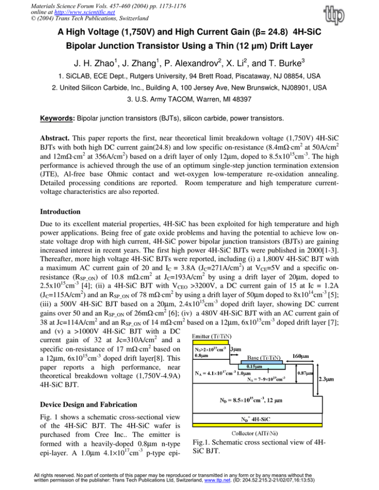
Fig. 1 shows a schematic cross-sectional view
of the 4H-SiC BJT. The 4H-SiC wafer is
purchased from Cree Inc.. The emitter is
formed with a heavily-doped 0.8µm n-type
epi-layer. A 1.0µm 4.1×1017cm-3 p-type epi-
Fig.1. Schematic cross sectional view of 4HSiC BJT.
All rights reserved. No part of contents of this paper may be reproduced or transmitted in any form or by any means without the
written permission of the publisher: Trans Tech Publications Ltd, Switzerland, www.ttp.net. (ID: 204.52.215.2-21/02/07,16:13:53)
1174
Silicon Carbide and Related Materials 2003
(a) An entire BJT cell.
(b)Emitter finger details
Fig.2. Top view of a fabricated 4H-SiC BJT.
layer is used as the base. The collector is a 12µm 8.5×1015cm-3 doped drift layer grown on n+-type
4H-SiC substrate. A single BJT cell is designed to contain 43 emitter fingers with the dimension of
1186µm×14µm. The device active area is 1.2mm2 excluding the bonding pads and the JTE region.
The total device dimension is 1.57mm×1.66mm. The designed spacing between the emitter-finger
edge and the base implanted region is 3µm. Fig.2 shows the top view photos of a fabricated 4H-SiC
BJT.
The emitter mesa is formed by using inductively coupled plasma (ICP) etching. The base contact
region is implanted by carbon and aluminum at room temperature with a total dose of Al and C
equals to 1.1×1015cm-2, which consists of C ions of 4x1014cm-2 at 28keV, 5.2x1014cm-2 at 60 keV,
and 1.1x1014cm-2 at 75 keV plus Al ions of 3.6x1014cm-2 at 50 keV and 7.5x1014cm-2 at 100 keV.
The implanted sample is then annealed at 1550oC for 30 minutes in Ar. A single step JTE based on
the p-type base epi-layer is used to improve the edge termination. The JTE region width is 160µm.
Each BJT cell is isolated from each other by a mesa etching of ~1.4µm into the drift layer. The
passivation is done first by a 2-hour wet thermal oxidation at 1100oC, followed by a 1-hour Ar
annealing at 1100oC. The sample is then annealed for 3 hours at 950oC for the wet-oxygen lowtemperature re-oxidation[9]. After thermal oxidation, 250nm SiO2 and 250nm Si3N4 are deposited
by PEVCD to increase the passivation layer thickness. Emitter and base contact is formed by 200nm
Ti covered by 200nm TiN, which is Al-free and is to prevent possible Al-spiking during the
following high temperature Ohmic contact annealing. AlTi(20nm)\Ni(700nm) bi-layer is used as
the collector contact metal on the substrate. All the contacts are annealed simultaneously in
hydrogen and nitrogen forming gas for 8 minutes at 1050oC. The emitter n-type specific contact
resistance is 6.5×10⁻⁶ Ω⋅cm2, and the base p-type specific contact resistance is 0.2 Ω⋅cm2. After the
Ohmic contact formation, another bi-layer of PECVD SiO2 (410nm) and Si3N4 (250nm) is deposited
for the insulation between the overlay metals. Finally the overlay metals of Ti(50nm) and Au(
1.5µm) are deposited to connect emitter fingers and to form the base and emitter bonding pads. The
collector overlay metal is 100nm Ni and 700nm Au on the substrate.
Characterization and Discussion
The forward I-V characteristics of the fabricated 4H-SiC BJT are measured by Tektronix 371A
curve tracer. The blocking performance is tested by Keithley 248 high voltage supply and Keithley
6517A electrometer. Fig.3 shows the I-V characteristics of a fabricated BJT at room temperature.
An open-base blocking voltage (VCEO) of 1750V with a low leakage current IC= 0.4µA is achieved,
Materials Science Forum Vols. 457-460
Fig.3. BJT I-V curves at room temperature.
1175
Fig.4. BJT I-V curves at 150oC.
together with a DC current gain of 24.8 for high collector current densities ranging from 230 to
270A/cm2. The AC current gain is 28 at around Jc=125A/cm2. IC is tested up to 4.92A
(JC=410A/cm2) at VCE=6.5V. The specific on-resistance (RSP_ON) is 12.0mΩ⋅cm2 based on IC=
4.27A (JC=356A/cm2) at VCE=4.26V. At a lower current density of 50A/cm2, the BJT has an RSP_ON
of only 8.4mΩcm2.
Negative temperature coefficient for the current gain is observed. Fig.4 shows the BJT I-V
curves measured at 150oC. The peak current gain decreases to 15.9 at Ic=2.38A(Jc=198A/cm2),
Vce=20V. The RSP_ON increases to 21.6 mΩ⋅cm2 based on IC= 2.1A (JC=175A/cm2) at VCE=3.78V.
The blocking voltage is slightly increased to VCEO=1760V with a leakage current of 4µA.
The BJT DC current gain at VCE=10V is shown in Fig.5 as a function of the collector current
density. At room temperature, the DC current gain is above 24.0 for Jc=160A/cm2 to Jc=319A/cm2.
The peak DC current gain is 24.8 and is maintained over the range of Jc=230A/cm2 to 270A/cm2.
At 150oC, it is seen that the BJT maintains a
DC current gain above 15 over a high current
density of JC=125A/cm2 to Jc=225A/cm2. The
value of VB2/RSP_ON for the BJT is 255MW/cm2
at Jc=356A/cm2 and 365MW/cm2 at
Jc=50A/cm2. This is among the best reported to
date[4,5].
The ideal parallel plane junction breakdown
voltage of this 12µm drift layer is 1856V. The
achieved experimental open-base blocking
voltage Vceo=1750V reaches 94% of the
theoretical value.
The high blocking
performance in this 12µm drift layer BJT is
attributed first to the optimum single-step JTE
for edge termination. Secondly, using the Alfree base Ohmic contact eliminates the possible
Al-spiking, and prevents the blocking
Fig.5. Current gain v.s. collector current
degradation due to Ohmic contact annealing [6density at room temperature and 150oC.
8]. And finally, the low-temperature wet-
Silicon Carbide and Related Materials 2003
1
-1
1.4x10
10
o
25 C
o
150 C
-1
1.4x10
-3
10
-3
10
-5
-5
10
-7
10
1.4x10
I(A)
2
oxygen re-oxidation annealing
could result in a better junction
passivation for both the base-emitter
junction and the base-collector
junction, and hence greatly reduces
the edge leakage currents. Fig. 6
presents the base-emitter junction
characteristics of the fabricated
1750V-4.9A BJT measured by
HP4145B Semiconductor parameter
analyzer, which shows a much less
leakage current compared to the
previously
reported
BJTs[3].
Switching characterization shows
that the BJT current rise and fall
times are less than 350ns.
J (A/cm )
1176
-7
1.4x10
-9
1.4x10
-9
1.4x10
-80
-11
-60
-40
-20
0
1
2
3
4
10
VBE (V)
Fig.6. Base-emitter junction characteristics.
Summary
A near theoretical high blocking voltage (1750V) 4H-SiC BJT has been demonstrated and tested to
4.9A (Jc=410A/cm2) by using a drift layer of only 12µm doped to 8.5×1015cm-3. The BJT achieves a
DC current gain of 24.8 over a wide range of high current densities. The lowest RSP_ON at room
temperature is 8.4mΩ⋅cm2 at 50A/cm2 and 12mΩ⋅cm2 at 356A/cm2. At 150oC ambient temperature,
the BJT maintains a DC current gain larger than 15 over the range of Jc=125A/cm2 to Jc=225A/cm2.
Further processing technologies improvements are needed to achieve higher current gains and
higher switching speed.
Acknowledgment
Authors at Rutgers University acknowledge financial support provided by United Silicon
Carbide(USC), Inc.. Authors at USC, Inc. acknowledge financial support provided by Army
TACOM SBIR program (Contract No. DAAE07-02-C-L050) managed by Dr. T. Burke.
References
[1]S.Ryu, A.K.Agarwal, R.Singh, J.W.Palmour: 58th IEEE Dev. Res. Conf. Digest, (2000), p.133.
[2]Y.Tang, J.B. Fedsion, T.P. Chow: 58th IEEE Dev. Res. Conf. Digest(2000), p.131.
[3]Y.Luo, L.Fursin, J.H.Zhao: IEE Elec. Lett. Vol. 36(17) (2000),p.1496.
[4]S.Ryu, A.K. Agarwal, R.Singh, J.W. Palmour, IEEE Elec. Dev. Lett., Vol.22, (2001), p124.
[5]C. Huang, J. A. Cooper Jr: IEEE ISPSD-2002, p.57, 2002.
[6]C-F Huang, J. A. Cooper, Jr.: 60th IEEE Dev. Res. Conf. Digest, (2002), p.183.
[7]J.Zhang, Y.Luo, P.Alexandrov, L.Fursin, and J.H.Zhao: IEEE Elec. Dev. Lett., Vol. 24
(2003),p.327.
[8]Y.Luo, J.Zhang, P.Alexandrov, L.Fursin, J.H.Zhao and T.Burke: IEEE Elec. Dev. Lett., under
reviewing.
[9] L.A.Lipkin, D.B.Slater, Jr., J.W. Palmour: Mater. Sci. Forum Vol.264-268(1998), p.853.
