Freescale Semiconductor, Inc.
Application Note
AN2528/D
Rev. 0, 5/2003
Standard Space Vector
Modulation TPU Function Set
(svmStd)
Freescale Semiconductor, Inc...
By Milan Brejl, Ph.D.
Functional Overview
Standard Space Vector Modulation (svmStd) is a technique that is used to
implement a straightforward method of switching motor windings in
applications such as AC induction motor control and PMSM motor control. The
function set consists of 5 TPU functions:
•
Standard Space Vector Modulation – Top (svmStd_top)
•
Standard Space Vector Modulation – Bottom (svmStd_bottom)
•
Synchronization Signal for Standard Space Vector Modulation
(svmStd_sync)
•
Resolver Reference Signal for Standard Space Vector Modulation
(svmStd_res)
•
Fault Input for Standard Space Vector Modulation (svmStd_fault)
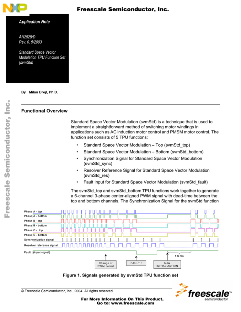
The svmStd_top and svmStd_bottom TPU functions work together to generate
a 6-channel 3-phase center-aligned PWM signal with dead-time between the
top and bottom channels. The Synchronization Signal for the svmStd function
Phase A - top
Phase A - bottom
Phase B - top
Phase B - bottom
Phase C - top
Phase C - bottom
Synchronization signal
Resolver reference signal
Fault (input signal)
1.6 m s
Change of
PW M period
FAU LT !
New
INITIALIZATIO N
Figure 1. Signals generated by svmStd TPU function set
© Freescale Semiconductor, Inc., 2004. All rights reserved.
For More Information On This Product,
Go to: www.freescale.com
© Motorola, Inc., 2003
Freescale Semiconductor, Inc.
AN2528/D
can be used to generate one or more adjustable signals for a wide range of
uses, that are synchronized to the PWM, and track changes in the PWM period.
The Resolver Reference Signal for the svmStd function can be used to
generate one or more 50% duty-cycle adjustable signals that are also
synchronized to the PWM.The Fault Input for the svmStd function is a TPU
input function that sets all PWM outputs low when the input signal goes low.
See Figure 1.
Freescale Semiconductor, Inc...
Function Set Configuration
None of the TPU functions in the Standard Space Vector Modulation TPU
function set can be used separately. The svmStd_top and svmStd_bottom
functions have to be used together. The svmStd_top is used on 3 channels, the
svmStd_bottom on a further 3 channels, and within each phase, the function
svmStd_top has to be assigned on a lower TPU channel than the function
svmStd_bottom. This is illustrated in the examples in Table 2 and Table 3. One
or more channels running a Synchronization Signal for svmStd as well as
Resolver Reference Signals for svmStd functions can be added to the
svmStd_top and svmStd_bottom functions. They can run with different settings
on each channel. The function Fault Input for svmStd can also be added to the
svmStd_top and svmStd_bottom functions. It is recommended to use it on
channel 15, and to select the hardware option that disables all TPU output pins
when the channel 15 input signal is low (DTPU bit = 1). This ensures that the
hardware reacts quickly to a pin fault state. Note that it is not only the PWM
channels, but all TPU output channels, including the synchronization signals,
that are disabled in this configuration.
Table 1 shows the configuration options and restrictions.
Table 1. svmStd TPU function set configuration options and restrictions
Optional/
Mandatory
How many
channels
svmStd_top
mandatory
3
svmStd_bottom
mandatory
3
svmStd_sync
svmStd_res
optional
optional
1 or more
1 or more
svmStd_fault
optional
1
TPU function
Assignable channels
any 3 channels, within each phase a
lower TPU channel than the same
phase svmStd_bottom
any 3 channels, within each phase a
higher TPU channel than the same
phase svmStd_top
any channels
any channels
any, recommended is 15 and DTPU bit
set
Table 2 and Table 3 show two examples of configuration.
2
Standard Space Vector Modulation TPU Function Set (svmStd)
For More Information On This Product,
Go to: www.freescale.com
Freescale Semiconductor, Inc.
AN2528/D
Function Set Configuration
Table 2. Example of configuration
Freescale Semiconductor, Inc...
Channel
0
1
2
3
4
5
10
15
TPU function
svmStd_top
svmStd_bottom
svmStd_top
svmStd_bottom
svmStd_top
svmStd_bottom
svmStd_sync
svmStd_fault
Priority
high
high
high
high
high
high
low
high
Table 3. Example of configuration
Channel
0
1
2
3
4
5
10
11
15
TPU function
svmStd_top
svmStd_top
svmStd_top
svmStd_bottom
svmStd_bottom
svmStd_bottom
svmStd_sync
svmStd_res
svmStd_fault
Priority
high
high
high
high
high
high
low
low
high
Table 4 shows the TPU function code sizes.
Table 4. TPU function code sizes
TPU function
svmStd_top
svmStd_bottom
svmStd_sync
svmStd_res
svmStd_fault
Configuration Order
Code size
16 µ instructions + 8 entries = 24 long words
197 µ instructions + 8 entries = 205 long words
26 µ instructions + 8 entries = 34 long words
38 µ instructions + 8 entries = 46 long words
9 µ instructions + 8 entries = 17 long words
The CPU configures the TPU as follows.
1. Disables the channels by clearing the two channel priority bits on each
channel used (not necessary after reset).
2. Selects the channel functions on all used channels by writing the
function numbers to the channel function select bits.
Standard Space Vector Modulation TPU Function Set (svmStd)
For More Information On This Product,
Go to: www.freescale.com
3
Freescale Semiconductor, Inc.
AN2528/D
3. Initializes function parameters. The parameters T, prescaler, DT, MPW,
SQRT3 and sync_presc_addr must be set before initialization. If an
svmStd_sync channel or an svmStd_res channel is used, then also its
parameters must be set before initialization.
Freescale Semiconductor, Inc...
4. Issues an HSR (Host Service Request) type %10 to one of the
svmStd_bottom channels to initialize all PWM channels. Issues an HSR
type %10 to the svmStd_sync channels, svmStd_res channels and
svmStd_fault channel, if used.
5. Enables servicing by assigning high, middle or low priority to the channel
priority bits. All PWM channels must be assigned the same priority to
ensure correct operation. The CPU must ensure that the svmStd_sync
or svmStd_res channels are initialized after the initialization of PWM
channels:
–
–
–
NOTE:
assign a priority to the PWM channels to enable their initialization
if a Synchronization Signal or a Resolver Reference Signal channel
is used, wait until the HSR bits are cleared to indicate that
initialization of the PWM channels has completed and
assign a priority to the svmStd_sync or svmStd_res channels to
enable their initialization
A CPU routine that configures the TPU can be generated automatically using
the MPC500_Quick_Start Graphical Configuration Tool.
Detailed Function Description
Standard Space
Vector Modulation –
Top (svmStd_top)
and Standard Space
Vector Modulation –
Bottom
(svmStd_bottom)
The svmStd_top and svmStd_bottom TPU functions work together to generate
a 6-channel, 3-phase PWM signal, with dead-time between the top and bottom
channels. In order to charge the bootstrap transistors, the PWM signals start to
run 1.6ms after their initialization (at 20MHz TCR1 clock). The functions
generate signals corresponding to Reference Voltage Vector Amplitude of 0
(50% duty-cycle) until the first reload values are processed.
The CPU controls the PWM output by setting the TPU parameters. The Stator
Reference Voltage Vector components uá and uâ have to be adjusted during
run time. The PWM period T and the prescaler – the number of PWM periods
per reload of new values – are also read at each reload, so these parameters
can be changed during run time. Conversely, dead-time (DT) and minimum
pulse width (MPW) are not supposed to be changed during run time. The CPU
notifies the TPU that the new reload values are prepared by setting the LD_OK
parameter. The TPU notifies the CPU that the reload values have been read
and new values can be written by clearing the LD_OK parameter.
The TPU writes the parameter Sector, which indicates the current Stator
Reference Voltage Vector position in sector 1 to 6.
4
Standard Space Vector Modulation TPU Function Set (svmStd)
For More Information On This Product,
Go to: www.freescale.com
Freescale Semiconductor, Inc.
AN2528/D
Detailed Function Description
The following figures show the input Stator Reference Voltage Vector
components uá and uâ, corresponding sectors and output PWM signal duty
cycle ratios:
amplitude
Components of the Stator Reference Voltage Vector
1
0.5
0
-0.5
0
60
120
180
240
300
360
angle
Standard Space Vector Modulation Technique
duty cycle ratios
Freescale Semiconductor, Inc...
-1
alpha
beta
1
0.9
0.8
0.7
0.6
0.5
0.4
0.3
0.2
0.1
0 0
Phase A
Phase B
Phase C
60
120
180
240
300
360
angle
Sector 1 Sector 2 Sector 3 Sector 4 Sector 5 Sector 6
Figure 2. Standard Space Vector Modulation Technique
The following equations describe how the Space Vector Modulation PWM
signal high-times htA, htB, htC and transition times tlow-high and thigh-low of each
channel are calculated:
U β = T ⋅ uβ
U α = T ⋅ uα
X =Uβ
Y=
Z=
U β + Uα 3
2
U β − Uα 3
Sector:
2
=
<
=! ; ;!
=
; V.
IV.
III.
VI.
<! ;!
I.
Standard Space Vector Modulation TPU Function Set (svmStd)
For More Information On This Product,
Go to: www.freescale.com
=! II.
5
Freescale Semiconductor, Inc.
AN2528/D
ht A = T + X2 − Z
Sector I., IV.:
ht B = T + X2 + Z = t A + Z
htC = T − X2 + Z = t B − X
htA = T +Y2 −Z
Sector II., V.:
htB = T +Y2 +Z = t A + Z
htC = T −Y2 −Z = t A − Y
Sector III., VI.: htA = T −X2+Y
Freescale Semiconductor, Inc...
htB = T +X2−Y = tC + X
htC = T −X2−Y = t A − Y
ht A
top channel
bottom channel
DT
DT
center_time
T
Phase A:
– top channel
ht A − DT
2
ht A − DT
= center_time +
2
t low-high = center_time −
t high-low
– bottom channel
ht A + DT
2
htA + DT
= center_time +
2
t high-low = center_time −
tlow-high
Phase B and Phase C similarly with htB and htC substituted to htA.
6
Standard Space Vector Modulation TPU Function Set (svmStd)
For More Information On This Product,
Go to: www.freescale.com
Freescale Semiconductor, Inc.
AN2528/D
Detailed Function Description
Host Interface
Written By CPU
Written by both CPU and TPU
Written By TPU
Not Used
Table 5. svmStd_top Control Bits
Name
3
2
1
0
Freescale Semiconductor, Inc...
Channel Function Select
1
0
Channel Priority
1
0
Host Service Bits (HSR)
1
Options
svmStd_top function number
(Assigned during assembly the
DPTRAM code from library TPU
functions)
00 – Channel Disabled
01 – Low Priority
10 – Middle Priority
11 – High Priority
00 – No Host Service Request
01 – Not used
10 – Not used
11 – Not used
0
Host Sequence Bits (HSQ)
xx – Not used
Channel Interrupt Enable
x – Not used
Channel Interrupt Status
x – Not used
0
0
Table 6. svmStd_bottom Control Bits
Name
3
2
1
0
Channel Function Select
1
0
Channel Priority
1
0
Host Service Bits (HSR)
Options
svmStd_bottom function number
(Assigned during assembly the
DPTRAM code from library TPU
functions)
00 – Channel Disabled
01 – Low Priority
10 – Middle Priority
11 – High Priority
00 – No Host Service Request
01 – Not used
10 – Initialization
11 – Stop
Standard Space Vector Modulation TPU Function Set (svmStd)
For More Information On This Product,
Go to: www.freescale.com
7
Freescale Semiconductor, Inc.
AN2528/D
Table 6. svmStd_bottom Control Bits
Name
1
0
Host Sequence Bits (HSQ)
xx – Not used
Channel Interrupt Enable
0 – Channel Interrupt Disabled
1 – Channel Interrupt Enabled
Channel Interrupt Status
0 – Interrupt Not Asserted
1 – Interrupt Asserted
0
0
Freescale Semiconductor, Inc...
Options
TPU function svmStd_bottom generates an interrupt when the current values
of Ualfa, Ubeta, T and prescaler have been read by the TPU, and indicates to
the CPU that it can write new variables. The CPU program can either wait for
this interrupt to occur, or poll the LD_OK bit to check it has cleared. The
interrupt is generated at each reload by one of the bottom channels. The top
channels do not generate any interrupts.
Table 7. svmStd_top and svmStd_bottom Parameter RAM
Phase A
bottom channel
Phase A
top channel
Channel
8
Parameter 15 14 13 12 11 10 9 8 7 6 5
0
htA
1
HLtime_AT
bottom_chan_A
2
center_time
3
4
LD_OK
Sector
5
6
7
fault_pinstate
0
LHtime_AB
HLtime_AB
1
2
UA
UB
3
Ualfa
4
5
Ubeta
6
7
Standard Space Vector Modulation TPU Function Set (svmStd)
For More Information On This Product,
Go to: www.freescale.com
4
3
2
1
0
Freescale Semiconductor, Inc.
AN2528/D
Detailed Function Description
Table 7. svmStd_top and svmStd_bottom Parameter RAM
Phase C
bottom channel
Phase C
top channel
Phase B
bottom channel
Freescale Semiconductor, Inc...
Phase B
top channel
Channel
Parameter 15 14 13 12 11 10 9 8 7 6 5
0
htB
HLtime_BT
1
2
bottom_chan_B
UA3
3
4
SQRT3
5
sync_presc_addr
6
7
0
LHtime_BB
HLtime_BB
1
2
T_copy
dec
3
T
4
5
prescaler
6
7
0
htC
HLtime_CT
1
bottom_chan_C
2
3
prsc_copy
4
5
6
7
0
LHtime_CB
1
HLtime_CB
min_ht
2
max_ht
3
4
DT
MPW
5
6
7
4
3
2
1
0
Table 8. svmStd_top and svmStd_bottom parameter description
Parameter
Ualfa, Ubeta
T
prescaler
Format
Description
Parameters written by CPU
Stator Reference Voltage Vector
16-bit fractional
components
PWM period in number of TCR1
16-bit unsigned integer
TPU cycles
The number of PWM periods per
16-bit unsigned integer
reload of new values
Standard Space Vector Modulation TPU Function Set (svmStd)
For More Information On This Product,
Go to: www.freescale.com
9
Freescale Semiconductor, Inc.
AN2528/D
Table 8. svmStd_top and svmStd_bottom parameter description
Freescale Semiconductor, Inc...
Parameter
Format
Description
Dead-time in number of TCR1
DT
16-bit unsigned integer
TPU cycles
Minimum pulse width in number of
MPW
16-bit unsigned integer
TCR1 TPU cycles. See
Performance for details.
sqrt(3)/2 = 0.866 = $6EDA
SQRT3
16-bit fractional
constant
address of synchronization
channel prescaler parameter:
$X4,
sync_presc_addr 8-bit unsigned integer
where X is synchronization
channel number.
$0 if no synchronization channel
is used.
Parameters written by both TPU and CPU
0 ... CPU can update variables
LD_OK
1-bit
1 ... TPU can read variables
CPU sets 1, TPU sets 0
Parameters written by TPU
The position of Stator Reference
Sector
16-bit unsigned integer
Voltage Vector in a sector. The
Sector can be 1, 2, 3, 4, 5 or 6
If fault channel is used, state of
fault pin:
fault_pinstate
0 or 1
0 ... low
1 ... high
Other parameters are just for TPU function inner use.
Performance
Table 9. svmStd_top State Statistics
State
HL
LH_C5
Max IMB Clock Cycles
2
28
RAM Accesses by TPU
1
10
Table 10. svmStd_bottom State Statistics
State
INIT
STOP
LH
HL
LH_RLD
10
Max IMB Clock Cycles
108
38
2
6
44
RAM Accesses by TPU
32
0
1
1
16
Standard Space Vector Modulation TPU Function Set (svmStd)
For More Information On This Product,
Go to: www.freescale.com
Freescale Semiconductor, Inc.
AN2528/D
Detailed Function Description
Table 10. svmStd_bottom State Statistics
State
C1
C2
C3
C4
Freescale Semiconductor, Inc...
NOTE:
Max IMB Clock Cycles
48
48
50
48
RAM Accesses by TPU
3
4
3
8
Execution times do not include the time slot transition time (TST = 10 or 14 IMB
clocks)
LH_C5
HL
- top
LH_C5
HL
Phase A
HL
LH
- bottom
HL
- top
HL
LH
LH_C5
LH_C5
HL
Phase B
- bottom
- top
HL
LH
LH_C5
HL
HL
LH
LH_C5
HL
Phase C
- bottom
HL
LH_RLD
LH_RLD
C1
C2
C3
C4
HL
flag0 = 1
center_time
center_time
T
T
not a reload period
reload period
Figure 3. svmStd_top and svmStd_bottom timing
NOTE:
The bottom channel with longest momentary low-time is marked by a flag0 and
runs the LH_RLD and C1, C2, C3, C4 states.
Standard Space Vector Modulation TPU Function Set (svmStd)
For More Information On This Product,
Go to: www.freescale.com
11
Freescale Semiconductor, Inc.
AN2528/D
HL
LH_C5
- top
Phase A
- bottom
- top
Phase B
- bottom
Freescale Semiconductor, Inc...
- top
Phase C
- bottom
flag0 = 1
LH
flag0 = 0
INIT
HL
no reload yet
flag0 = 1
LH_RLD
reload
C1234
STOP
4th-time
3-times
HSR = 10
HSR = 11
Figure 4. svmStd_top and svmStd_bottom state diagram
Minimum Pulse Width
The TPU cannot generate PWM signals with duty cycle ratios very close to 0%
or 100%. The minimum pulse width that the TPU can be guaranteed to correctly
generate is determined by the TPU function itself and by the activity on the
other channels. When the TPU function is requested to generate a narrower
pulse a collision can occur. To prevent this, the parameter MPW (minimum
pulse width) is introduced. The TPU functions svmStd_top and svmStd_bottom
limit the narrowest generated pulse widths to MPW. The CPU program should
check, and limit, the maximum amplitude of the Stator Reference Voltage
Vector before decomposition to uá, uâ components. The maximum amplitude of
the Stator Reference Voltage Vector should be less than
1−
2 ( MPW + DT )
T
If this is not the case, the TPU function will start to limit the minimum pulse
widths to MPW to prevent a collision, and the duty cycle ratio traces will be
deformed as shown on Figure 5.
12
Standard Space Vector Modulation TPU Function Set (svmStd)
For More Information On This Product,
Go to: www.freescale.com
Freescale Semiconductor, Inc.
Freescale Semiconductor, Inc...
duty cycle ratios
AN2528/D
Detailed Function Description
Standard Space Vector Modulation Technique - limitation
1
0.9
0.8
0.7
0.6
0.5
0.4
Phase A
0.3
Phase B
0.2
Phase C
0.1
0 0
60
120
180
240
300
360
Figure 5. Effect of limitation
The MPW is written by the CPU. The MPW depends on the whole TPU unit
configuration, especially the lengths of the longest states of other functions,
and their priorities, running on the same TPU. The MPW has to be correctly
calculated at the time the whole TPU unit is configured.
top channel
LH_C5
DT
bottom channel
latency
center_time
HL
MPW
Figure 6. Timing of the worst case
When svmStd_top and svmStd_bottom are running alone on one TPU, the
minimum pulse width can be calculated according to Figure 6. This illustrates
the worst case timing. The bottom channel low to high transition runs the HL
state that sets the following high to low transition. The HL state lasts 6 IMB
clock cycles (see Table 10). Each state is preceded by the Time Slot Transition
(TST), which takes 10 IMB clock cycles. So the time necessary to set the next
transition on the bottom channel is 16 IMB clock cycles. In addition, there is a
latency between the low to high transition and the start of the HL state. The top
channel state LH_C5, which is serviced at the time, causes the latency. The
LH_C5 state lasts 28 IMB clock cycles (see Table 9). Its time slot transition is
Standard Space Vector Modulation TPU Function Set (svmStd)
For More Information On This Product,
Go to: www.freescale.com
13
Freescale Semiconductor, Inc.
AN2528/D
10 IMB clock cycles. The service starts immediately after the top channel high
to low transition, which occurs at a period of DT before the bottom channel low
to high transition (see Figure 6), so that the latency is 28 IMB clock cycles + 10
IMB clock cycles – DT. The svmStd functions are designed so that no other
svmStd state can request service at this time. The MPW, in the case when only
svmStd functions are running on one TPU, is then
latency + 16 IMB clock cycles =
= 28 IMB clock cycles + 10 IMB clock cycles – DT + 16 IMB clock cycles =
= 54 IMB clock cycles – DT
Freescale Semiconductor, Inc...
and is a minimum at least 16 IMB clock cycles (when latency = 0).
Note that the MPW, as well as the DT, are not entered into the parameter RAM
in IMB clock cycles, but in TCR1 clock cycles. It is recommended for the
svmStd function that the TCR1 clck is configured for its maximum speed, which
is the IMB clock divided by 2. In this case the MPW = 27 – DT, with a minimum
value of 8.
When other functions are running together on the same TPU as the svmStd
functions, the latency could be lengthened. To maintain sufficiently high
performance of svmStd, it is recommended that the following rules are followed
to configure the TPU:
•
assign svmStd PWM channels high priority
•
assign svmStd PWM functions on low channel numbers so that no other
function with high priority is assigned a channel with a lower number
In this instance, one of the two worst case timing cases can happen. These are
illustrated in Figure 7 and Figure 8. Which case occurs depends on the DT.
time slot sequence
TST
H
M
TST+4
H
TST
L
TST+4
H
LH_C5
top channel
bottom channel
TST
DT
latency
HL
MPW
Figure 7. Worst case timing – case one
14
Standard Space Vector Modulation TPU Function Set (svmStd)
For More Information On This Product,
Go to: www.freescale.com
Freescale Semiconductor, Inc.
AN2528/D
Detailed Function Description
time slot sequence
TST
H
TST
M
TST+4
TST+4
L
TST
H
TST
M or L
TST+4
H
LH_C5
top channel
DT
bottom channel
Freescale Semiconductor, Inc...
H
latency
HL
MPW
Figure 8. Worst case timing – case two
The time slot sequences at the top of both figures shows when a state of a high
(H), middle (M) or low (L) priority is serviced in the worst case. To calculate the
MPW follow these steps:
•
Get the lengths of the longest states.
– It is necessary to know the lengths of the longest states within all
functions of each priority group. The initialization states are not
considered – only the running states. Let's denote H as the time
period of the longest state within all functions running on high priority
(Do not consider svmStd functions). Let's denote M as the time
period of the longest state within all functions running on middle
priority and L as the time period of the longest state within all
functions running on low priority.
•
Decide which case of timing can occure.
– The first case can occure when the DT (in IMB clock cycles) is less
than TST + H + TST + M + TST+4 + LH_C5 + TST+4 + L (see Figure
8) that is 4*TST + 8 + H + M + L + LH_C5 that is 76 + H + M + L IMB
clock cycles.
if DT (in IMB clock cycles) < 76 + H + M + L
then – case one
else – case two
•
Calculate MPW based on case one or case two.
– In case one the MPW is (according to Figure 7)
TST + H + TST + M + TST+4 + LH_C5 + TST + L + TST+4 + HL – DT
that is 92 + H + M + L – DT IMB clock cycles.
MPW (in IMB clock cycles) = 92 + H + M + L – DT
Standard Space Vector Modulation TPU Function Set (svmStd)
For More Information On This Product,
Go to: www.freescale.com
15
Freescale Semiconductor, Inc.
AN2528/D
–
In case two the MPW is (according to Figure 8)
TST + H + TST + max(M,L) + TST+4 + HL
that is 40 + H + max(M,L) IMB clock cycles.
MPW (in IMB clock cycles) = 40 + H + max(M,L)
•
Convert MPW in IMB clock cycles to MPW in TCR1 clock cycles based
on TCR1 prescaler settings.
Freescale Semiconductor, Inc...
When there are no channels of middle or low priority, simply leave out all the H
or L and the following TST or TST+4 from the formulas.
When the recommended configuration rules are not adhered to, the timing of
the worst case is considerably more complicated. It requires some familiarity
with the details of the TPU priority scheme. In this case, the Worst-Case
Latency (WCL), which is automatically calculated by the MPC500_Quick_Start
Graphical Configuration Tool, can serve as a good approximation. This is
always longer than the real-case. Let the WCL be calculated after the
configuration of TPU channels and then find the longest WCL value within all
svmStd PWM channels. Convert the number, from IMB clock cycles to TCR1
clock cycles, to get the MPW.
Synchronization
signal for Standard
Space Vector
Modulation
(svmStd_sync)
16
The svmStd_sync TPU function uses information obtained from svmStd PWM
functions, the actual PWM center times and the PWM periods. This allows a
signal to be generated, which tracks the changes in the PWM period and is
always synchronized with the PWM. The synchronization signal is a positive
pulse generated repeatedly after the prescaler or presc_copy PWM periods
(see next paragraph). The low to high transition of the pulse can be adjusted
by a parameter, either negative or positive, to go a number of TCR1 TPU cycles
before or after the PWM period center time. The pulse width pw is another
synchronization signal parameter.
Standard Space Vector Modulation TPU Function Set (svmStd)
For More Information On This Product,
Go to: www.freescale.com
Freescale Semiconductor, Inc.
AN2528/D
Detailed Function Description
move > 0
prescaler = 1
pw
|move|
center_time
center_time
T
T
move < 0
prescaler = 2
Freescale Semiconductor, Inc...
pw
|move|
center_time
center_time
center_time
T
T
T
Figure 9. Synchronization signal adjustment examples
Synchronized Change
of PWM Prescaler
And Synchronization
Signal Prescaler
The svmStd_sync TPU function actually uses the presc_copy parameter
instead of the prescaler parameter. The prescaler parameter holds the
prescaler value that is copied to the presc_copy by the svmStd_bottom function
at the time the PWM parameters are reloaded. This ensures that new prescaler
values for the PWM signals, as well as the synchronization signal, are applied
at the same time. Write the synchronization signal prescaler parameter
address to the sync_presc_addr parameter to enable this mechanism. Write 0
to disable it, and remember to set the synchronization signal presc_copy
parameter instead of the prescaler parameter in this case.
Host Interface
Written By CPU
Written by both CPU and TPU
Written By TPU
Not Used
Table 11. svmStd_sync Control Bits
Name
3
2
1
0
Channel Function Select
1
0
Channel Priority
Options
svmStd_sync function number
(Assigned during assembly the
DPTRAM code from library TPU
functions)
00 – Channel Disabled
01 – Low Priority
10 – Middle Priority
11 – High Priority
Standard Space Vector Modulation TPU Function Set (svmStd)
For More Information On This Product,
Go to: www.freescale.com
17
Freescale Semiconductor, Inc.
AN2528/D
Table 11. svmStd_sync Control Bits
Name
1
0
Host Service Bits (HSR)
1
0
Host Sequence Bits (HSQ)
xx – Not used
Channel Interrupt Enable
0 – Channel Interrupt Disabled
1 – Channel Interrupt Enabled
Channel Interrupt Status
0 – Interrupt Not Asserted
1 – Interrupt Asserted
0
Freescale Semiconductor, Inc...
Options
00 – No Host Service Request
01 – Not used
10 – Initialization
11 – Not used
0
TPU function svmStd_sync generates an interrupt after each low to high
transition.
Table 12. svmStd_sync Parameter RAM
Synchronization channel
Channel
Parameter 15 14 13 12 11 10 9 8 7 6
0
move
1
pw
prescaler
2
presc_copy
3
4
time
dec
5
T_copy
6
5
4
3
2
1
0
7
Table 13. svmStd_sync parameter description
Parameter
move
pw
18
Format
Description
Parameters written by CPU
The number of TCR1 TPU cycles to
forego (negative) or come after
16-bit signed integer
(positive) the PWM period center
time
Synchronization pulse width in
16-bit unsigned integer
number of TCR1 TPU cycles.
Standard Space Vector Modulation TPU Function Set (svmStd)
For More Information On This Product,
Go to: www.freescale.com
Freescale Semiconductor, Inc.
AN2528/D
Detailed Function Description
Table 13. svmStd_sync parameter description
Freescale Semiconductor, Inc...
Parameter
Description
The number of PWM periods per
synchronization pulse
prescaler
16-bit unsigned integer
– use in case of synchronized
prescalers change
The number of PWM periods per
synchronization pulse
presc_copy
16-bit unsigned integer
– use in case of asynchronized
prescalers change
Parameters written by TPU
Other parameters are just for TPU function inner use.
Performance
Format
There is one limitation. The absolute value of parameter move has to be less
than a quarter of the PWM period T.
move <
T
4
Table 14. svmStd_sync State Statistics
State
INIT
S1
S2
S3
NOTE:
S1
Max IMB Clock Cycles
12
12
8
16
RAM Accesses by TPU
5
6
3
7
Execution times do not include the time slot transition time (TST = 10 or 14 IMB
clocks)
S2
S3
S1
center_time
center_time
center_time
T
T
T
S2
Figure 10. svmStd_sync timing
Standard Space Vector Modulation TPU Function Set (svmStd)
For More Information On This Product,
Go to: www.freescale.com
19
Freescale Semiconductor, Inc.
AN2528/D
HSR = 10
Freescale Semiconductor, Inc...
INIT
S1
S3
S2
Figure 11. svmStd_sync state diagram
Resolver Reference
Signal for Standard
Space Vector
Modulation
(svmStd_res)
The svmStd_res TPU function uses information read from the svmStd PWM
functions, the actual PWM center times and the PWM periods. This allows a
signal to be generated, which tracks the changes of the PWM period and is
always synchronized with the PWM. The resolver reference signal is a 50%
duty-cycle signal with a period equal to prescaler or synchronization channel
presc_copy PWM periods (see next paragraph). The low to high transition of
the pulse can be adjusted by a parameter, either negative or positive, to go a
number of TCR1 TPU cycles before or after the PWM period center time.
move > 0
prescaler = 1
|move|
center_time
center_time
T
T
center_time
center_time
center_time
T
T
T
move < 0
prescaler = 2
|move|
Figure 12. Resolver reference signal adjustment examples
20
Standard Space Vector Modulation TPU Function Set (svmStd)
For More Information On This Product,
Go to: www.freescale.com
Freescale Semiconductor, Inc.
AN2528/D
Detailed Function Description
Synchronized Change
of PWM Prescaler
And Resolver
Reference Signals
Prescaler
The svmStd_res TPU function can inherit the Synchronization Signal prescaler
that is synchronously changed with the PWM prescaler. Write the
synchronization signals presc_copy parameter address to the presc_addr
parameter to enable this mechanism. Write 0 to disable it, and in this case set
the prescaler parameter to directly specify prescaler value.
Freescale Semiconductor, Inc...
Host Interface
Written By CPU
Written by both CPU and TPU
Written By TPU
Not Used
Table 15. svmStd_res Control Bits
Name
3
2
1
0
Channel Function Select
1
0
Channel Priority
1
0
Host Service Bits (HSR)
1
Options
svmStd_res function number
(Assigned during assembly the
DPTRAM code from library TPU
functions)
00 – Channel Disabled
01 – Low Priority
10 – Middle Priority
11 – High Priority
00 – No Host Service Request
01 – Not used
10 – Initialization
11 – Not used
0
Host Sequence Bits (HSQ)
xx – Not used
Channel Interrupt Enable
x – Not used
Channel Interrupt Status
x – Not used
0
0
Standard Space Vector Modulation TPU Function Set (svmStd)
For More Information On This Product,
Go to: www.freescale.com
21
Freescale Semiconductor, Inc.
AN2528/D
Table 16. svmStd_res Parameter RAM
Freescale Semiconductor, Inc...
Resolver
Channel
Parameter 15 14 13 12 11 10 9 8 7 6
0
move
1
2
presc_addr
3
prescaler
time
4
dec
5
6
T_copy
7
5
4
3
2
1
0
Table 17. svmStd_res parameter description
Parameter
move
presc_addr
Format
Description
Parameters written by CPU
The number of TCR1 TPU cycles to
forego (negative) or come after
16-bit signed integer
(positive) the PWM period center
time
$00X6, where X is a number of
Synchronization Signal channel, to
inherit Sync. channel prescaler
or
16-bit unsigned integer
$0000 to enable direct specification
of prescaler value in prescaler
parameter
The number of PWM periods per
synchronization pulse
– use when apresc_addr = 0
Parameters written by TPU
Other parameters are just for TPU function inner use.
prescaler
Performance
1, 2, 4, 6, 8, 10, 12, 14, ...
There is one limitation. The absolute value of parameter move has to be less
than a quarter of the PWM period T.
move <
22
T
4
Standard Space Vector Modulation TPU Function Set (svmStd)
For More Information On This Product,
Go to: www.freescale.com
Freescale Semiconductor, Inc.
AN2528/D
Detailed Function Description
Table 18. svmStd_res State Statistics
State
INIT
S1
S3
Freescale Semiconductor, Inc...
NOTE:
Max IMB Clock Cycles
12
26
18
RAM Accesses by TPU
5
9
7
Execution times do not include the time slot transition time (TST = 10 or 14 IMB
clocks)
S3
S1
S1
center_time
center_time
center_time
T
T
T
Figure 13. svmStd_res timing
HSR = 10
INIT
S1
S3
Figure 14. svmStd_res state diagram
Fault Input for
Standard Space
Vector Modulation
(svmStd_fault)
The svmStd_fault is an input TPU function that monitors the pin, and if a high
to low transition occurs, immediately sets all PWM channels low and cancels
all further transitions on them. The PWM channels, as well as the
synchronization and resolver reference signal channels (if used), have to be
initialized again to start them running.
Standard Space Vector Modulation TPU Function Set (svmStd)
For More Information On This Product,
Go to: www.freescale.com
23
Freescale Semiconductor, Inc.
AN2528/D
The function returns the actual pinstate as a value of 0 (low) or 1 (high) in the
parameter fault_pinstate. The parameter is placed on the Phase A – top
channel to keep the fault channel parameter space free.
Host Interface
Written By CPU
Written by both CPU and TPU
Written By TPU
Not Used
Table 19. svmStd_fault Control Bits
Freescale Semiconductor, Inc...
Name
3
2
1
0
Channel Function Select
1
0
Channel Priority
1
0
Host Service Bits (HSR)
1
Options
svmStd_fault function number
(Assigned during assembly the
DPTRAM code from library TPU
functions)
00 – Channel Disabled
01 – Low Priority
10 – Middle Priority
11 – High Priority
00 – No Host Service Request
01 – Not used
10 – Initialization
11 – Not used
0
Host Sequence Bits (HSQ)
xx – Not used
Channel Interrupt Enable
0 – Channel Interrupt Disabled
1 – Channel Interrupt Enabled
Channel Interrupt Status
0 – Interrupt Not Asserted
1 – Interrupt Asserted
0
0
TPU function svmStd_fault generates an interrupt when a high to low transition
appears.
24
Standard Space Vector Modulation TPU Function Set (svmStd)
For More Information On This Product,
Go to: www.freescale.com
Freescale Semiconductor, Inc.
AN2528/D
Detailed Function Description
Table 20. svmStd_fault Parameter RAM
Freescale Semiconductor, Inc...
Fault input
Channel
Parameter 15 14 13 12 11 10 9
0
1
2
3
4
5
6
7
8
7
6
5
4
3
2
1
0
Table 21. svmStd_fault parameter description
Parameter
Format
Description
Table 22Parameters written by TPU
fault_pinstate
0 or 1
State of fault pin:
0 ... low
1 ... high
Performance
Table 23. svmStd_fault State Statistics
State
INIT
FAULT
NO_FAULT
NOTE:
Max IMB Clock Cycles
8
44
4
RAM Accesses by TPU
2
1
1
Execution times do not include the time slot transition time (TST = 10 or 14 IMB
clocks)
Standard Space Vector Modulation TPU Function Set (svmStd)
For More Information On This Product,
Go to: www.freescale.com
25
Freescale Semiconductor, Inc.
AN2528/D
NO_FAULT
FAULT
Figure 15. svmStd_fault timing
HSR = 10
Freescale Semiconductor, Inc...
INIT
FAULT
NO_FAULT
Figure 16. svmStd_fault state diagram
26
Standard Space Vector Modulation TPU Function Set (svmStd)
For More Information On This Product,
Go to: www.freescale.com
Freescale Semiconductor, Inc.
Freescale Semiconductor, Inc...
AN2528/D
Detailed Function Description
Standard Space Vector Modulation TPU Function Set (svmStd)
For More Information On This Product,
Go to: www.freescale.com
27
Freescale Semiconductor, Inc.
How to Reach Us:
Home Page:
www.freescale.com
Freescale Semiconductor, Inc...
E-mail:
support@freescale.com
USA/Europe or Locations Not Listed:
Freescale Semiconductor
Technical Information Center, CH370
1300 N. Alma School Road
Chandler, Arizona 85224
+1-800-521-6274 or +1-480-768-2130
support@freescale.com
Europe, Middle East, and Africa:
Freescale Halbleiter Deutschland GmbH
Technical Information Center
Schatzbogen 7
81829 Muenchen, Germany
+44 1296 380 456 (English)
+46 8 52200080 (English)
+49 89 92103 559 (German)
+33 1 69 35 48 48 (French)
support@freescale.com
Japan:
Freescale Semiconductor Japan Ltd.
Headquarters
ARCO Tower 15F
1-8-1, Shimo-Meguro, Meguro-ku,
Tokyo 153-0064
Japan
0120 191014 or +81 3 5437 9125
support.japan@freescale.com
Asia/Pacific:
Freescale Semiconductor Hong Kong Ltd.
Technical Information Center
2 Dai King Street
Tai Po Industrial Estate
Tai Po, N.T., Hong Kong
+800 2666 8080
support.asia@freescale.com
For Literature Requests Only:
Freescale Semiconductor Literature Distribution Center
P.O. Box 5405
Denver, Colorado 80217
1-800-441-2447 or 303-675-2140
Fax: 303-675-2150
LDCForFreescaleSemiconductor@hibbertgroup.com
AN2528/D
Rev. 0
5/2003
Information in this document is provided solely to enable system and software
implementers to use Freescale Semiconductor products. There are no express or
implied copyright licenses granted hereunder to design or fabricate any integrated
circuits or integrated circuits based on the information in this document.
Freescale Semiconductor reserves the right to make changes without further notice to
any products herein. Freescale Semiconductor makes no warranty, representation or
guarantee regarding the suitability of its products for any particular purpose, nor does
Freescale Semiconductor assume any liability arising out of the application or use of
any product or circuit, and specifically disclaims any and all liability, including without
limitation consequential or incidental damages. “Typical” parameters which may be
provided in Freescale Semiconductor data sheets and/or specifications can and do
vary in different applications and actual performance may vary over time. All operating
parameters, including “Typicals” must be validated for each customer application by
customer’s technical experts. Freescale Semiconductor does not convey any license
under its patent rights nor the rights of others. Freescale Semiconductor products are
not designed, intended, or authorized for use as components in systems intended for
surgical implant into the body, or other applications intended to support or sustain life,
or for any other application in which the failure of the Freescale Semiconductor product
could create a situation where personal injury or death may occur. Should Buyer
purchase or use Freescale Semiconductor products for any such unintended or
unauthorized application, Buyer shall indemnify and hold Freescale Semiconductor
and its officers, employees, subsidiaries, affiliates, and distributors harmless against all
claims, costs, damages, and expenses, and reasonable attorney fees arising out of,
directly or indirectly, any claim of personal injury or death associated with such
unintended or unauthorized use, even if such claim alleges that Freescale
Semiconductor was negligent regarding the design or manufacture of the part.
For More Information On This Product,
Go to: www.freescale.com
